JAJSP64I December   2003  – October 2024 OPA695

PRODUCTION DATA  

  1.   1
  2. 特長
  3. アプリケーション
  4. 概要
  5. Pin Configuration and Functions
  6. Specifications
    1. 5.1  Absolute Maximum Ratings
    2. 5.2  ESD Ratings
    3. 5.3  Recommended Operating Conditions
    4. 5.4  Thermal Information
    5. 5.5  Electrical Characteristics VS = ±5 V, OPA695ID, OPA695IDBV
    6. 5.6  Electrical Characteristics VS = 5 V, OPA695ID, OPA695IDBV
    7. 5.7  Electrical Characteristics VS = ±5 V, OPA695IDGK
    8. 5.8  Electrical Characteristics VS = 5 V, OPA695IDGK
    9. 5.9  Typical Characteristics: VS = ±5 V, OPA695IDBV, OPA695ID
    10. 5.10 Typical Characteristics: VS = 5 V, OPA695IDBV, OPA695ID
    11. 5.11 Typical Characteristics: VS = ±5 V, OPA695IDGK
    12. 5.12 Typical Characteristics: VS = 5 V, OPA695IDGK
  7. Detailed Description
    1. 6.1 Overview
    2. 6.2 Functional Block Diagram
    3. 6.3 Feature Description
      1. 6.3.1 Wideband Current-Feedback Operation
      2. 6.3.2 Input and ESD Protection
    4. 6.4 Device Functional Modes
  8. Application and Implementation
    1. 7.1 Application Information
      1. 7.1.1 Operating Suggestions
        1. 7.1.1.1 Setting Resistor Values to Optimize Bandwidth
        2. 7.1.1.2 Output Current and Voltage
        3. 7.1.1.3 Driving Capacitive Loads
        4. 7.1.1.4 Distortion Performance
        5. 7.1.1.5 Noise Performance
        6. 7.1.1.6 Thermal Analysis
      2. 7.1.2 LO Buffer Amplifier
      3. 7.1.3 Wideband Cable Driving Applications
        1. 7.1.3.1 Cable Modem Return Path Driver
        2. 7.1.3.2 Arbitrary Waveform Driver
      4. 7.1.4 Differential I/O Applications
    2. 7.2 Typical Application
      1. 7.2.1 Design Requirements
        1. 7.2.1.1 Saw Filter Buffer
      2. 7.2.2 Detailed Design Procedure
      3. 7.2.3 Application Curve
    3. 7.3 Power Supply Recommendations
    4. 7.4 Layout
      1. 7.4.1 Layout Guidelines
      2. 7.4.2 Layout Example
  9. Device and Documentation Support
    1. 8.1 Device Support
      1. 8.1.1 Design-In Tools
        1. 8.1.1.1 Demonstration Fixtures
    2. 8.2 Documentation Support
      1. 8.2.1 Related Documentation
    3. 8.3 ドキュメントの更新通知を受け取る方法
    4. 8.4 サポート・リソース
    5. 8.5 Trademarks
    6. 8.6 静電気放電に関する注意事項
    7. 8.7 用語集
  10. Revision History
  11. 10Mechanical, Packaging, and Orderable Information

Typical Characteristics: VS = ±5 V, OPA695IDGK

at G = +8 V/V, RF = 402 Ω, and RL = 100 Ω (unless otherwise noted)
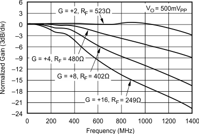
OPA695 Noninverting Small-Signal Frequency Response
 
Figure 5-39 Noninverting Small-Signal Frequency Response
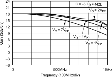
OPA695 Noninverting Large-Signal Frequency Response
 
Figure 5-41 Noninverting Large-Signal Frequency Response
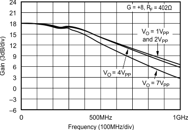
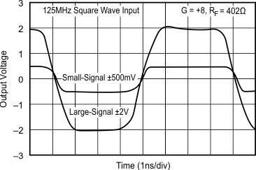
OPA695 Noninverting Large- and Small-Signal Frequency Responses
 
Figure 5-43 Noninverting Large- and Small-Signal Frequency Responses
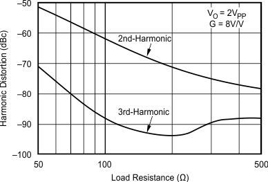
OPA695 10-MHz Harmonic Distortion vs Load Resistance
 
Figure 5-45 10-MHz Harmonic Distortion vs Load Resistance
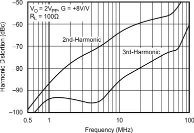
OPA695 Harmonic Distortion vs Frequency
 
Figure 5-47 Harmonic Distortion vs Frequency
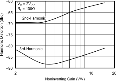
OPA695 10-MHz Harmonic Distortion vs Noninverting Gain
 
Figure 5-49 10-MHz Harmonic Distortion vs Noninverting Gain
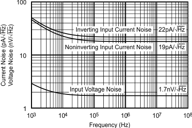
OPA695 Input
                        Voltage and Current Noise Density
 
Figure 5-51 Input Voltage and Current Noise Density
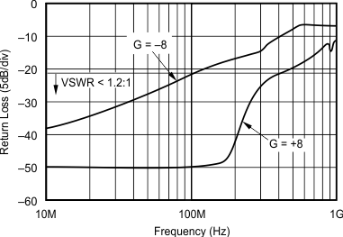
OPA695 Input
                        Return Loss vs Frequency (S11)
 
Figure 5-53 Input Return Loss vs Frequency (S11)
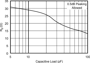
OPA695 RS vs Capacitive Load
 
Figure 5-55 RS vs Capacitive Load
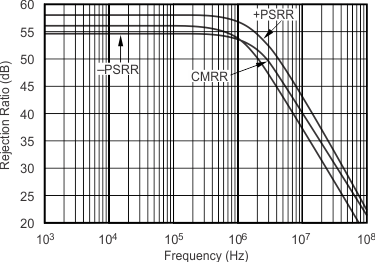
OPA695 CMRR
                        and PSRR vs Frequency
 
Figure 5-57 CMRR and PSRR vs Frequency
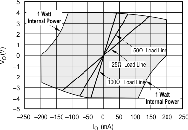
OPA695 Output Voltage and Current Limitations
 
Figure 5-59 Output Voltage and Current Limitations
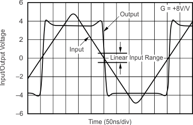
OPA695 Noninverting Overdrive Recovery
 
Figure 5-61 Noninverting Overdrive Recovery
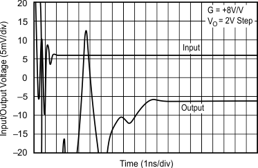
OPA695 Settling Time
 
Figure 5-63 Settling Time
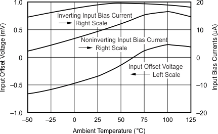
OPA695 Typical DC Drift Over Temperature
 
Figure 5-65 Typical DC Drift Over Temperature
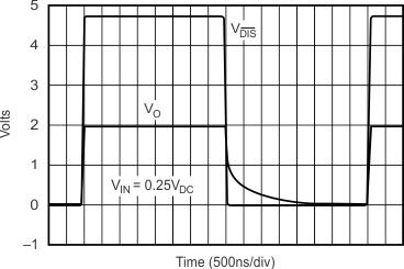
OPA695 Large-Signal Disable and Enable Responses
 
Figure 5-67 Large-Signal Disable and Enable Responses
OPA695 Inverting Small-Signal Frequency Response
 
Figure 5-40 Inverting Small-Signal Frequency Response
OPA695 Inverting Large-Signal Frequency Response
 
Figure 5-42 Inverting Large-Signal Frequency Response
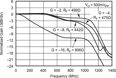
OPA695 Inverting Large- and Small-Signal Frequency Responses
 
Figure 5-44 Inverting Large- and Small-Signal Frequency Responses
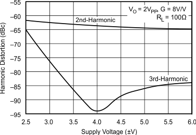
OPA695 10-MHz Harmonic Distortion vs Supply Voltage
 
Figure 5-46 10-MHz Harmonic Distortion vs Supply Voltage
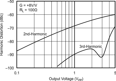
OPA695 10-MHz Harmonic Distortion vs Output Voltage
 
Figure 5-48 10-MHz Harmonic Distortion vs Output Voltage
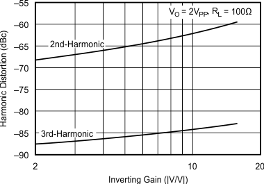
OPA695 10-MHz Harmonic Distortion vs Inverting Gain
 
Figure 5-50 10-MHz Harmonic Distortion vs Inverting Gain
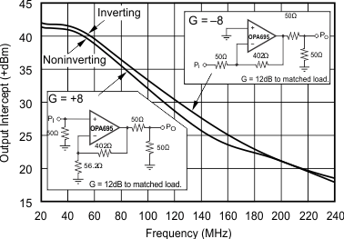
OPA695 Two-Tone 3rd-Order Intermodulation Intercept
 
Figure 5-52 Two-Tone 3rd-Order Intermodulation Intercept
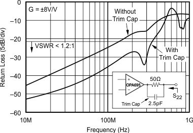
OPA695 Output Return Loss vs Frequency (S22)
 
Figure 5-54 Output Return Loss vs Frequency (S22)
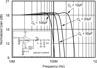
OPA695 Small-Signal Frequency Response vs Capacitive Load
 
Figure 5-56 Small-Signal Frequency Response vs Capacitive Load
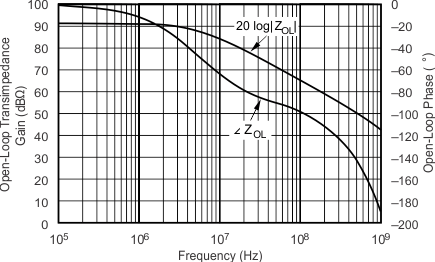
OPA695 Open-Loop Transimpedance Gain and Phase
 
Figure 5-58 Open-Loop Transimpedance Gain and Phase
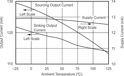
OPA695 Supply and Output Current vs Temperature
 
Figure 5-60 Supply and Output Current vs Temperature
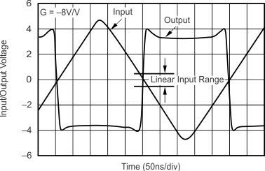
OPA695 Inverting Overdrive Recovery
 
Figure 5-62 Inverting Overdrive Recovery
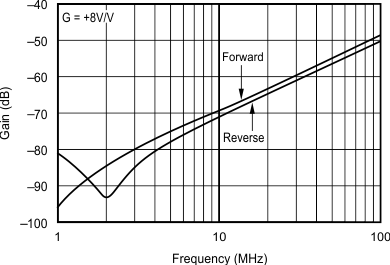
OPA695 Disabled Feedthrough vs Frequency
 
Figure 5-64 Disabled Feedthrough vs Frequency
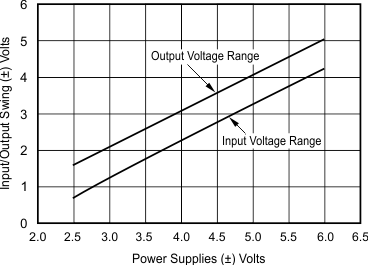
OPA695 Common-Mode Input and Output Swing vs Supply Voltage
 
Figure 5-66 Common-Mode Input and Output Swing vs Supply Voltage
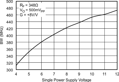
OPA695 Small-Signal BW vs Single-Supply Voltage
 
Figure 5-68 Small-Signal BW vs Single-Supply Voltage