JAJSP64I December 2003 – October 2024 OPA695
PRODUCTION DATA
- 1
- 1 特長
- 2 アプリケーション
- 3 概要
- 4 Pin Configuration and Functions
-
5 Specifications
- 5.1 Absolute Maximum Ratings
- 5.2 ESD Ratings
- 5.3 Recommended Operating Conditions
- 5.4 Thermal Information
- 5.5 Electrical Characteristics VS = ±5 V, OPA695ID, OPA695IDBV
- 5.6 Electrical Characteristics VS = 5 V, OPA695ID, OPA695IDBV
- 5.7 Electrical Characteristics VS = ±5 V, OPA695IDGK
- 5.8 Electrical Characteristics VS = 5 V, OPA695IDGK
- 5.9 Typical Characteristics: VS = ±5 V, OPA695IDBV, OPA695ID
- 5.10 Typical Characteristics: VS = 5 V, OPA695IDBV, OPA695ID
- 5.11 Typical Characteristics: VS = ±5 V, OPA695IDGK
- 5.12 Typical Characteristics: VS = 5 V, OPA695IDGK
- 6 Detailed Description
- 7 Application and Implementation
- 8 Device and Documentation Support
- 9 Revision History
- 10Mechanical, Packaging, and Orderable Information
6.3.1 Wideband Current-Feedback Operation
The OPA695 provides a new level of performance in wideband current-feedback operational amplifiers. The nearly constant ac performance over a wide gain range, along with 5000-V/μs slew rate and ultra-low distortion makes this device an excellent choice for high-speed data acquisition gain stages. While optimized at a gain of +8 V/V (12 dB to a matched 50-Ω load) to give 600-MHz bandwidth, applications from gains of 1 V/V to 40 V/V can be supported. At gains above 20 V/V, the signal bandwidth starts to decrease, but still exceeds 180 MHz up to a gain of 40 V/V (26 dB to a matched 50-Ω load). Single +5-V supply operation is also supported with similar bandwidths but reduced output power capability.
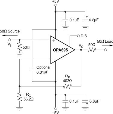
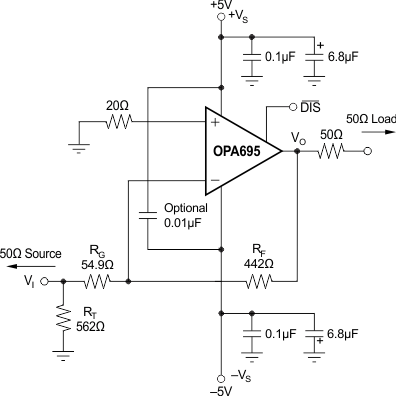
Figure 6-1 shows the dc-coupled, gain of +8 V/V, dual-power supply circuit used as the basis of the ±5-V specifications and typical characteristic curves. The total effective load is 100 Ω || 458 Ω = 82 Ω. The disable control line ( DIS) is typically left open for normal amplifier operation. Assert the disable line low to shut off the OPA695. Figure 6-2 shows the dc-coupled, gain of –8 V/V, dual-power supply circuit used as the basis of the inverting typical characteristic curves. Inverting operation offers several performance benefits. There is no common-mode signal across the input stage; therefore, the distortion performance is slightly improved. In addition to the usual power-supply decoupling capacitors to ground, a 0.01-μF capacitor is included between the two power-supply pins. In practical PCB layouts, this optional added capacitor typically improves the 2nd-harmonic distortion performance by 3 dB to 6 dB for bipolar-supply operation.
 Figure 6-1 DC-Coupled, G = +8 V/V, Bipolar Supply Specifications and Test Circuit
 Figure 6-2 DC-Coupled, G = –8 V/V, Bipolar Supply Specifications and Test Circuit