JAJSPW5C November   2023  – May 2024 LMKDB1104 , LMKDB1108 , LMKDB1120 , LMKDB1204

PRODUCTION DATA  

  1.   1
  2. 特長
  3. アプリケーション
  4. 概要
  5. Device Comparison
  6. Pin Configuration and Functions
  7. Specifications
    1. 6.1 Absolute Maximum Ratings
    2. 6.2 ESD Ratings
    3. 6.3 Recommended Operating Conditions
    4. 6.4 Thermal Information
    5. 6.5 Electrical Characteristics
    6. 6.6 SMBus Timing Requirements
    7. 6.7 SBI Timing Requirements
    8. 6.8 Timing Diagrams
    9. 6.9 Typical Characteristics
  8. Parameter Measurement Information
  9. Detailed Description
    1. 8.1 Overview
    2. 8.2 Functional Block Diagram
    3. 8.3 Feature Description
      1. 8.3.1 Input Features
        1. 8.3.1.1 Running Input Clocks When Device is Powered Off
        2. 8.3.1.2 Fail-Safe Inputs
        3. 8.3.1.3 Input Configurations
          1. 8.3.1.3.1 Internal Termination for Clock Inputs
          2. 8.3.1.3.2 AC-Coupled or DC-Coupled Clock Inputs
      2. 8.3.2 Flexible Power Sequence
        1. 8.3.2.1 PWRDN# Assertion and Deassertion
        2. 8.3.2.2 OE# Assertion and Deassertion
        3. 8.3.2.3 PWRGD Assertion
        4. 8.3.2.4 Clock Input and PWRGD/PWRDN# Behaviors When Device Power is Off
      3. 8.3.3 LOS and OE
        1. 8.3.3.1 Additional OE# Pins for LMKDB1120 and Backward Compatibility
        2. 8.3.3.2 Synchronous OE
        3. 8.3.3.3 OE Control
        4. 8.3.3.4 Automatic Output Disable
        5. 8.3.3.5 LOS Detection
      4. 8.3.4 Output Features
        1. 8.3.4.1 Double Termination
        2. 8.3.4.2 Programmable Output Slew Rate
        3. 8.3.4.3 Programmable Output Swing
        4. 8.3.4.4 Accurate Output Impedance
        5. 8.3.4.5 Programmable Output Impedance
    4. 8.4 Device Functional Modes
      1. 8.4.1 SMBus Mode
      2. 8.4.2 SBI Mode
      3. 8.4.3 Pin Mode
  10. Register Maps
    1. 9.1 LMKDB1120 Registers
    2. 9.2 LMKDB1108 Registers
    3. 9.3 LMKDB1204 Registers
  11. 10Application and Implementation
    1. 10.1 Application Information
    2. 10.2 Typical Application
      1. 10.2.1 Design Requirements
      2. 10.2.2 Detailed Design Procedure
      3. 10.2.3 Application Curves
    3. 10.3 Power Supply Recommendations
    4. 10.4 Layout
      1. 10.4.1 Layout Guidelines
      2. 10.4.2 Layout Example
  12. 11Device and Documentation Support
    1. 11.1 Documentation Support
      1. 11.1.1 Related Documentation
    2. 11.2 ドキュメントの更新通知を受け取る方法
    3. 11.3 サポート・リソース
    4. 11.4 Trademarks
    5. 11.5 静電気放電に関する注意事項
    6. 11.6 用語集
  13. 12Revision History
  14. 13Mechanical, Packaging, and Orderable Information

SMBus Mode

In SMBus mode, LMKDB11xx device SMBus registers can be written and read through SMBus pins. Pin SADR1 and SADR0 set the SMBus address.

SADR1 SADR0 8-Bit SMBus Address (R/W Bit = 0)
Low Low 0xD8
Low Float 0xDA
Low High 0xDE
Float Low 0xC2
Float Float 0xC4
Float High 0xC6
High Low 0xCA
High Float 0xCC
High High 0xCE

Table 8-5 Command Code Definition
BIT DESCRIPTION
7 0 = Block Read or Block Write operation
1 = Byte Read or Byte Write operation
(6:0) Register address for Byte operations, or starting register address for Block, operations
LMKDB1108 LMKDB1120 LMKDB1204  Generic
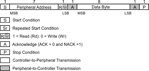
          Programming Sequence Figure 8-7 Generic Programming Sequence
LMKDB1108 LMKDB1120 LMKDB1204  Byte Write
          Protocol Figure 8-8 Byte Write Protocol
LMKDB1108 LMKDB1120 LMKDB1204  Byte Read
          Protocol Figure 8-9 Byte Read Protocol
LMKDB1108 LMKDB1120 LMKDB1204  Block Write
          Protocol Figure 8-10 Block Write Protocol
LMKDB1108 LMKDB1120 LMKDB1204  Block Read
          Protocol Figure 8-11 Block Read Protocol