JAJSQB5H June   1998  – July 2024 SN74AHCT174

PRODMIX  
  1.   1
  2. 特長
  3. アプリケーション
  4. 概要
  5. Pin Configuration and Functions
  6. Specifications
    1. 5.1 Absolute Maximum Ratings
    2. 5.2 ESD Ratings
    3. 5.3 Recommended Operating Conditions
    4. 5.4 Thermal Information
    5. 5.5 Electrical Characteristics
    6. 5.6 Timing Requirements
    7. 5.7 Switching Characteristics
    8. 5.8 Noise Characteristics
    9. 5.9 Operating Characteristics
  7. Parameter Measurement Information
  8. Detailed Description
    1. 7.1 Overview
    2. 7.2 Functional Block Diagram
    3. 7.3 Device Functional Modes
  9. Application and Implementation
    1. 8.1 Power Supply Recommendations
    2. 8.2 Layout
      1. 8.2.1 Layout Guidelines
      2. 8.2.2 Layout Example
  10. Device and Documentation Support
    1. 9.1 Documentation Support (Analog)
      1. 9.1.1 Related Documentation
    2. 9.2 ドキュメントの更新通知を受け取る方法
    3. 9.3 サポート・リソース
    4. 9.4 Trademarks
    5. 9.5 静電気放電に関する注意事項
    6. 9.6 用語集
  11. 10Revision History
  12. 11Mechanical, Packaging, and Orderable Information

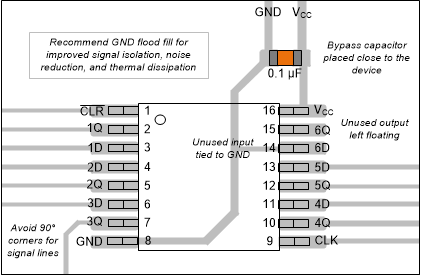
Layout Example

SN74AHCT174 Example layout for the
                    SN74AHCT174  in the PW package. Figure 8-1 Example layout for the SN74AHCT174 in the PW package.