JAJSQB5H June 1998 – July 2024 SN74AHCT174
PRODMIX
4 Pin Configuration and Functions
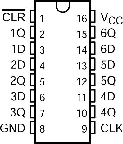
 Figure 4-1 Package SN74AHCT174 D, DB,
DGV, N, NS, or PW Package (Top View)
Figure 4-1 Package SN74AHCT174 D, DB,
DGV, N, NS, or PW Package (Top View)Table 4-1 Pin Functions
| PIN | I/O(1) | DESCRIPTION | |
|---|---|---|---|
| NO. | NAME | ||
| 1 | CLR | I | Clear all channels, active low |
| 2 | 1Q | O | Channel 1, Q output |
| 3 | 1D | I | Channel 1, D input |
| 4 | 2D | I | Channel 2, D input |
| 5 | 2Q | O | Channel 2, Q output |
| 6 | 3D | I | Channel 3, D input |
| 7 | 3Q | O | Channel 3, Q output |
| 8 | GND | — | Ground |
| 9 | CLK | I | Clock all channels, rising edge triggered |
| 10 | 4Q | O | Channel 4, Q output |
| 11 | 4D | I | Channel 4, D input |
| 12 | 5Q | O | Channel 5, Q output |
| 13 | 5D | I | Channel 5, D input |
| 14 | 6D | I | Channel 6, D input |
| 15 | 6Q | O | Channel 6, Q output |
| 16 | VCC | — | Positive supply |