JAJSQC4C august 2015 – may 2023 ISO5852S
PRODUCTION DATA
- 1
- 1 特長
- 2 アプリケーション
- 3 概要
- 4 Revision History
- 5 概要 (続き)
- 6 Pin Configuration and Function
-
7 Specifications
- 7.1 Absolute Maximum Ratings
- 7.2 ESD Ratings
- 7.3 Recommended Operating Conditions
- 7.4 Thermal Information
- 7.5 Power Ratings
- 7.6 Insulation Specifications
- 7.7 Safety-Related Certifications
- 7.8 Safety Limiting Values
- 7.9 Electrical Characteristics
- 7.10 Switching Characteristics
- 7.11 Insulation Characteristics Curves
- 7.12 Typical Characteristics
- 8 Parameter Measurement Information
- 9 Detailed Description
-
10Application and Implementation
- 10.1 Application Information
- 10.2
Typical Applications
- 10.2.1 Design Requirements
- 10.2.2
Detailed Design Procedure
- 10.2.2.1 Recommended ISO5852S Application Circuit
- 10.2.2.2 FLT and RDY Pin Circuitry
- 10.2.2.3 Driving the Control Inputs
- 10.2.2.4 Local Shutdown and Reset
- 10.2.2.5 Global-Shutdown and Reset
- 10.2.2.6 Auto-Reset
- 10.2.2.7 DESAT Pin Protection
- 10.2.2.8 DESAT Diode and DESAT Threshold
- 10.2.2.9 Determining the Maximum Available, Dynamic Output Power, POD-max
- 10.2.2.10 Example
- 10.2.2.11 Higher Output Current Using an External Current Buffer
- 10.2.3 Application Curves
- 11Power Supply Recommendations
- 12Layout
- 13Device and Documentation Support
- 14Mechanical, Packaging, and Orderable Information
10.2.2.2 FLT and RDY Pin Circuitry
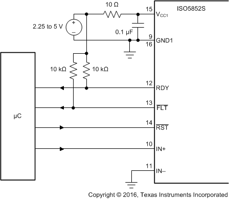
A is 50-kΩ pullup resistor exists internally on FLT and RDY pins. The FLT and RDY pins are an open-drain output. A 10-kΩ pullup resistor can be used to make it faster rise and to provide logic high when FLT and RDY is inactive, as shown in Figure 10-4.
Fast common-mode transients can inject noise and glitches on FLT and RDY pins because of parasitic coupling. The injection of noise and glitches is dependent on board layout. If required, additional capacitance (100 pF to 300 pF) can be included on the FLT and RDY pins.
 Figure 10-4 FLT and RDY Pin Circuitry for High CMTI