JAJSRJ5A October   2023  – April 2024 SN74LVC2G100-Q1

PRODUCTION DATA  

  1.   1
  2. 特長
  3. アプリケーション
  4. 概要
  5. Pin Configuration and Functions
  6. 仕様
    1. 5.1 Absolute Maximum Ratings
    2. 5.2 ESD Ratings
    3. 5.3 Recommended Operating Conditions
    4. 5.4 Thermal Information
    5. 5.5 Electrical Characteristics
    6. 5.6 Switching Characteristics
    7. 5.7 Timing Characteristics
    8. 5.8 Noise Characteristics
    9. 5.9 Typical Characteristics
  7. Parameter Measurement Information
  8. Detailed Description
    1. 7.1 Overview
    2. 7.2 Functional Block Diagram
    3. 7.3 Feature Description
      1. 7.3.1 CMOS Schmitt-Trigger Inputs
      2. 7.3.2 Balanced CMOS Push-Pull Outputs
      3. 7.3.3 Clamp Diode Structure
      4. 7.3.4 Wettable Flanks
    4. 7.4 Device Functional Modes
    5. 7.5 Combinatorial Logic Configurations
  9. アプリケーションと実装
    1. 8.1 Application Information
    2. 8.2 Typical Application
      1. 8.2.1 Design Requirements
        1. 8.2.1.1 Power Considerations
        2. 8.2.1.2 Input Considerations
        3. 8.2.1.3 Output Considerations
      2. 8.2.2 Detailed Design Procedure
      3. 8.2.3 Application Curves
    3. 8.3 Power Supply Recommendations
    4. 8.4 Layout
      1. 8.4.1 Layout Guidelines
      2. 8.4.2 Layout Example
  10. デバイスおよびドキュメントのサポート
    1. 9.1 ドキュメントのサポート
      1. 9.1.1 関連資料
    2. 9.2 ドキュメントの更新通知を受け取る方法
    3. 9.3 サポート・リソース
    4. 9.4 商標
    5. 9.5 静電気放電に関する注意事項
    6. 9.6 用語集
  11. 10Revision History
  12. 11メカニカル、パッケージ、および注文情報

Clamp Diode Structure

Figure 7-1 shows the inputs and outputs to this device have negative clamping diodes only.

CAUTION: Voltages beyond the values specified in the Absolute Maximum Ratings table can cause damage to the device. The input and output voltage ratings may be exceeded if the input and output clamp-current ratings are observed.
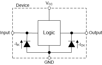
SN74LVC2G100-Q1 Electrical Placement of
                    Clamping Diodes for Each Input and OutputFigure 7-1 Electrical Placement of Clamping Diodes for Each Input and Output