JAJSRP9 September   2024

ADVANCE INFORMATION  

  1.   1
  2. 特長
  3. アプリケーション
  4. 説明
  5. Device Options
  6. Pin Configuration and Functions
  7. Specifications
    1. 6.1 Absolute Maximum Rating
    2. 6.2 ESD Ratings
    3. 6.3 Recommended Operating Conditions
    4. 6.4 Thermal Information
    5. 6.5 Electrical Characteristics
    6. 6.6 I2C Interface Timing Characteristics
    7. 6.7 Typical Characteristics
  8. Detailed Description
    1. 7.1 Overview
    2. 7.2 Functional Block Diagram
    3. 7.3 Feature Description
      1. 7.3.1 Pulse Frequency Modulation (PFM)
      2. 7.3.2 Forced PWM Mode
      3. 7.3.3 Low Dropout Operation (100% Duty Cycle)
      4. 7.3.4 Soft Start
      5. 7.3.5 Switch Current Limit and HICCUP Short-Circuit Protection
      6. 7.3.6 Undervoltage Lockout
      7. 7.3.7 Thermal Warning and Shutdown
    4. 7.4 Device Functional Modes
      1. 7.4.1 Enable and Disable (EN)
      2. 7.4.2 Output Discharge
      3. 7.4.3 Power Good (PG)
      4. 7.4.4 Voltage Setting and Mode Selection (VSET/MODE)
    5. 7.5 Programming
      1. 7.5.1 Serial Interface Description
      2. 7.5.2 Standard-, Fast-, and Fast-Mode Plus Protocol
      3. 7.5.3 HS Mode Protocol
      4. 7.5.4 I2C Update Sequence
      5. 7.5.5 I2C Register Reset
  9. Register Map
    1. 8.1 Target Address Byte
    2. 8.2 Register Address Byte
    3. 8.3 VOUT Register 1
    4. 8.4 VOUT Register 2
    5. 8.5 CONTROL Register
    6. 8.6 STATUS Register
  10. Application and Implementation
    1. 9.1 Application Information
    2. 9.2 Typical Application
      1. 9.2.1 Design Requirements
      2. 9.2.2 Detailed Design Procedure
        1. 9.2.2.1 Custom Design With WEBENCH® Tools
        2. 9.2.2.2 Setting The Output Voltage
        3. 9.2.2.3 Output Filter Design
        4. 9.2.2.4 Inductor Selection
        5. 9.2.2.5 Capacitor Selection
      3. 9.2.3 Application Curves
    3. 9.3 Power Supply Recommendations
    4. 9.4 Layout
      1. 9.4.1 Layout Guidelines
      2. 9.4.2 Layout Example
        1. 9.4.2.1 Thermal Considerations
  11. 10Device and Documentation Support
    1. 10.1 Device Support
      1. 10.1.1 サード・パーティ製品に関する免責事項
      2. 10.1.2 Development Support
        1. 10.1.2.1 Custom Design With WEBENCH® Tools
    2. 10.2 Documentation Support
      1. 10.2.1 Related Documentation
    3. 10.3 ドキュメントの更新通知を受け取る方法
    4. 10.4 サポート・リソース
    5. 10.5 Trademarks
    6. 10.6 静電気放電に関する注意事項
    7. 10.7 用語集
  12. 11Revision History
  13. 12Mechanical, Packaging, and Orderable Information
    1. 12.1 Tape and Reel Information

Soft Start

After enabling the device, there is a 700µs (typical) enable delay (tdelay) before the device starts switching. After the enable delay, if the SS pin is left un-connected an internal soft start-up circuitry controls the output voltage ramp up with a period of 1.5ms (tRamp) for TPS6286A06 and with 500us for TP6286A08, TPS6286A10, TPS6286B08, and TPS6286B10. Leaving the SS pin disconnected provides the fastest start-up ramp. This action avoids excessive inrush current and creates a smooth output voltage rise-slope. This action also prevents excessive voltage drops of primary cells and rechargeable batteries with high internal impedance. The device is able to start into a prebiased output capacitor. The device starts with the applied bias voltage and ramps the output voltage to the nominal value. An external soft-start capacitor connected from SS to GND is charged 20µA by an internal current source during soft start until it reaches the reference voltage of 0.9V. The capacitance required to set a certain ramp-time (tramp) therefore is:

Equation 3. C S S = 20 µA × t r a m p m s 0.9 V

If the device is set to shutdown (EN = GND), undervoltage lockout, or thermal shutdown, an internal resistor pulls the SS pin to GND to make sure of a proper low level. Returning from those states causes a new start-up sequence.
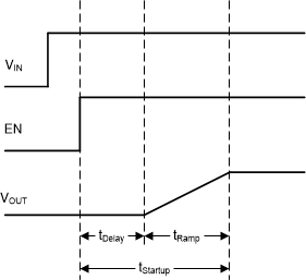
TPS6286A06 TPS6286B10 Start-up SequenceFigure 7-3 Start-up Sequence