JAJSRU9B October   2023  – August 2024 TMCS1133

PRODUCTION DATA  

  1.   1
  2. 特長
  3. アプリケーション
  4. 概要
  5. Device Comparison
  6. Pin Configuration and Functions
  7. Specifications
    1. 6.1 Absolute Maximum Ratings
    2. 6.2 ESD Ratings
    3. 6.3 Recommended Operating Conditions
    4. 6.4 Thermal Information
    5. 6.5 Insulation Specifications
    6. 6.6 Electrical Characteristics
    7. 6.7 Typical Characteristics
  8. Parameter Measurement Information
    1. 7.1 Accuracy Parameters
      1. 7.1.1 Sensitivity Error
      2. 7.1.2 Offset Error and Offset Error Drift
      3. 7.1.3 Nonlinearity Error
      4. 7.1.4 Power Supply Rejection Ratio
      5. 7.1.5 Common-Mode Rejection Ratio
      6. 7.1.6 External Magnetic Field Errors
    2. 7.2 Transient Response Parameters
      1. 7.2.1 CMTI, Common-Mode Transient Immunity
    3. 7.3 Safe Operating Area
      1. 7.3.1 Continuous DC or Sinusoidal AC Current
      2. 7.3.2 Repetitive Pulsed Current SOA
      3. 7.3.3 Single Event Current Capability
  9. Detailed Description
    1. 8.1 Overview
    2. 8.2 Functional Block Diagram
    3. 8.3 Feature Description
      1. 8.3.1 Current Input
      2. 8.3.2 Ambient Field Rejection
      3. 8.3.3 High-Precision Signal Chain
        1. 8.3.3.1 Temperature Stability
        2. 8.3.3.2 Lifetime and Environmental Stability
      4. 8.3.4 Internal Reference Voltage
      5. 8.3.5 Current-Sensing Measurable Ranges
      6. 8.3.6 Overcurrent Detection
      7. 8.3.7 Sensor Diagnostics
    4. 8.4 Device Functional Modes
      1. 8.4.1 Power-Down Behavior
  10. Application and Implementation
    1. 9.1 Application Information
      1. 9.1.1 Total Error Calculation Examples
        1. 9.1.1.1 Room-Temperature Error Calculations
        2. 9.1.1.2 Full-Temperature Range Error Calculations
    2. 9.2 Typical Application
      1. 9.2.1 Design Requirements
      2. 9.2.2 Detailed Design Procedure
      3. 9.2.3 Application Curve
    3. 9.3 Power Supply Recommendations
    4. 9.4 Layout
      1. 9.4.1 Layout Guidelines
      2. 9.4.2 Layout Example
  11. 10Device and Documentation Support
    1. 10.1 Device Nomenclature
    2. 10.2 Device Support
      1. 10.2.1 Development Support
    3. 10.3 Documentation Support
      1. 10.3.1 Related Documentation
    4. 10.4 ドキュメントの更新通知を受け取る方法
    5. 10.5 サポート・リソース
    6. 10.6 Trademarks
    7. 10.7 静電気放電に関する注意事項
    8. 10.8 用語集
  12. 11Revision History
  13. 12Mechanical, Packaging, and Orderable Information

Sensitivity Error

Sensitivity is the proportional change in the sensor output voltage due to a change in the input conductor current. This sensitivity is the slope of the first-order transfer function of the sensor (see Figure 7-1). The sensitivity of the TMCS1133 is tested and calibrated at the factory for high accuracy.
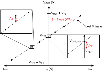
TMCS1133 Sensitivity,
                                        Offset, and Nonlinearity Error Figure 7-1 Sensitivity, Offset, and Nonlinearity Error

Sensitivity error eS is the deviation from ideal sensitivity and is defined in Equation 2 as the variation of the best-fit measured sensitivity from the ideal sensitivity.

Equation 2. eS=Sfit-SidealSideal

where

  • eS is the sensitivity error.
  • Sfit is the best fit sensitivity.
  • SIdeal is the ideal sensitivity.

Sensitivity thermal drift Sdrift,therm is the change in sensitivity with temperature and is reported in ppm/°C. To calculate sensitivity error at any given temperature T use Equation 3 to multiply the sensitivity thermal drift by the change in temperature from 25°C and add that value to the sensitivity error at 25°C.

Equation 3. e S , T = e S , 25 + S d r i f t , t h e r m × T

where

  • Sdrift,therm is the sensitivity drift over temperature in ppm/°C.
  • ΔT is the change in device temperature from 25°C.

Sensitivity lifetime drift Sdrift,life is the change in sensitivity due to operational and environmental stresses over the entire lifetime of the device, and is reported as a worst-case percentage change in sensitivity over lifetime at 25°C.