JAJSSU1 September 2024 LMR51425-Q1 , LMR51435-Q1
PRODUCTION DATA
- 1
- 1 特長
- 2 アプリケーション
- 3 概要
- 4 Device Comparison Table
- 5 Pin Configuration and Functions
- 6 Specifications
-
7 Detailed Description
- 7.1 Overview
- 7.2 Functional Block Diagram
- 7.3
Feature Description
- 7.3.1 Fixed Frequency Peak Current Mode Control
- 7.3.2 Adjustable Output Voltage
- 7.3.3 Enable
- 7.3.4 Switching Frequency
- 7.3.5 Power-Good Flag Output
- 7.3.6 Minimum ON-Time, Minimum OFF-Time, and Frequency Foldback
- 7.3.7 Bootstrap Voltage
- 7.3.8 Overcurrent and Short-Circuit Protection
- 7.3.9 Soft Start
- 7.3.10 Thermal Shutdown
- 7.4 Device Functional Modes
- 8 Application and Implementation
- 9 Device and Documentation Support
- 10Revision History
- 11Mechanical, Packaging, and Orderable Information
8.2 Typical Application
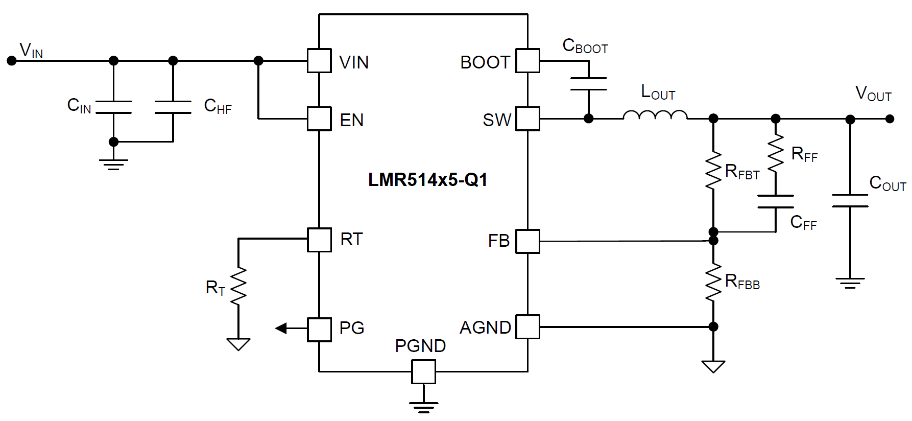
The LMR514x5-Q1 only requires a few external components to convert from a wide voltage range supply to a fixed output voltage. Figure 8-1 shows a basic schematic.
 Figure 8-1 Application Circuit
The external components have to fulfill the needs of the application and the stability criteria of the control loop of the device. Use the following tables to simplify the output filter component selection.
Table 8-1 L and COUT Typical Values for LMR51425-Q1
| fSW (kHz) | VOUT (V) | L (µH) | COUT (µF) (1) | RFBT (kΩ) | RFBB (kΩ) | CFF (pF) | RFF (kΩ) |
|---|---|---|---|---|---|---|---|
| 440 | 3.3 | 6.8 | 56 | 100 | 31.6 | 27 | 1 |
| 5 | 8.2 | 33 | 100 | 19.1 | 27 | 1 | |
| 1000 | 3.3 | 3.3 | 27 | 100 | 31.6 | 18 | 1 |
| 5 | 4.7 | 18 | 100 | 19.1 | 18 | 1 |
(1) A ceramic capacitor is used in this table. All the COUT values are after derating.
Table 8-2 L and COUT Typical Values for LMR51435-Q1
| fSW (kHz) | VOUT (V) | L (µH) | COUT (µF) (1) | RFBT (kΩ) | RFBB (kΩ) | CFF (pF) | RFF (kΩ) |
|---|---|---|---|---|---|---|---|
| 440 | 3.3 | 4.7 | 75 | 100 | 31.6 | 27 | 1 |
| 5 | 6.8 | 47 | 100 | 19.1 | 27 | 1 | |
| 1000 | 3.3 | 2.7 | 39 | 100 | 31.6 | 18 | 1 |
| 5 | 3.3 | 27 | 100 | 19.1 | 18 | 1 |
(1) A ceramic capacitor is used in this table. All the COUT values are after derating.