JAJSU80 March 2024
ADVANCE INFORMATION
- 1
- 1 特長
- 2 アプリケーション
- 3 概要
- 4 Device Comparison
-
5 Terminal Configuration and Functions
- 5.1 Pin Diagrams
- 5.2 Pin Attributes
- 5.3
Signal Descriptions
- 13
- 5.3.1 CPSW3G
- 5.3.2 CPTS
- 5.3.3 CSI-2
- 5.3.4 DDRSS
- 5.3.5 DSI
- 5.3.6 DSS
- 5.3.7 ECAP
- 5.3.8 Emulation and Debug
- 5.3.9 EPWM
- 5.3.10 EQEP
- 5.3.11 GPIO
- 5.3.12 GPMC
- 5.3.13 I2C
- 5.3.14 MCAN
- 5.3.15 MCASP
- 5.3.16 MCSPI
- 5.3.17 MDIO
- 5.3.18 MMC
- 5.3.19 OLDI
- 5.3.20 OSPI
- 5.3.21 Power Supply
- 5.3.22 Reserved
- 5.3.23 SERDES
- 5.3.24 System and Miscellaneous
- 5.3.25 TIMER
- 5.3.26 UART
- 5.3.27 USB
- 5.4 Pin Connectivity Requirements
-
6 Specifications
- 6.1 Absolute Maximum Ratings
- 6.2 ESD Ratings for AEC - Q100 Qualified Devices in the AMW Package
- 6.3 Power-On Hours (POH)
- 6.4 Recommended Operating Conditions
- 6.5 Operating Performance Points
- 6.6
Electrical
Characteristics
- 6.6.1 I2C Open-Drain, and Fail-Safe (I2C OD FS) Electrical Characteristics
- 6.6.2 Fail-Safe Reset (FS RESET) Electrical Characteristics
- 6.6.3 High-Frequency Oscillator (HFOSC) Electrical Characteristics
- 6.6.4 Low-Frequency Oscillator (LFXOSC) Electrical Characteristics
- 6.6.5 SDIO Electrical Characteristics
- 6.6.6 LVCMOS Electrical Characteristics
- 6.6.7 CSI-2 (D-PHY) Electrical Characteristics
- 6.6.8 USB2PHY Electrical Characteristics
- 6.6.9 DDR Electrical Characteristics
- 6.7 VPP Specifications for One-Time Programmable (OTP) eFuses
- 6.8 Thermal Resistance Characteristics
- 6.9
Timing and Switching Characteristics
- 6.9.1 Timing Parameters and Information
- 6.9.2 Power Supply Requirements
- 6.9.3 System Timing
- 6.9.4 Clock Specifications
- 6.9.5
Peripherals
- 6.9.5.1 ATL
- 6.9.5.2 CPSW3G
- 6.9.5.3 CPTS
- 6.9.5.4 CSI-2
- 6.9.5.5 CSI-2 TX
- 6.9.5.6 DDRSS
- 6.9.5.7 DSS
- 6.9.5.8 ECAP
- 6.9.5.9 Emulation and Debug
- 6.9.5.10 EPWM
- 6.9.5.11 EQEP
- 6.9.5.12 GPIO
- 6.9.5.13 GPMC
- 6.9.5.14 I2C
- 6.9.5.15 MCAN
- 6.9.5.16 MCASP
- 6.9.5.17 MCSPI
- 6.9.5.18 MMCSD
- 6.9.5.19 OSPI
- 6.9.5.20 PCIe
- 6.9.5.21 Timers
- 6.9.5.22 UART
- 6.9.5.23 USB
- 7 Detailed Description
-
8 Applications,
Implementation, and Layout
- 8.1 Device Connection and Layout Fundamentals
- 8.2 Peripheral- and Interface-Specific Design Information
- 8.3 Clock Routing Guidelines
- 9 Device and Documentation Support
- 10Revision History
- 11Mechanical, Packaging, and Orderable Information
6.9.5.7 DSS
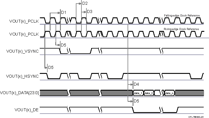
Table 6-43, Table 6-44, Figure 6-36, Table 6-45 and Figure 6-37 present timing conditions, requirements, and switching characteristics for DSS.
Table 6-43 DSS Timing Conditions
| PARAMETER | MIN | MAX | UNIT | |
|---|---|---|---|---|
| INPUT CONDITIONS | ||||
| SRI | Input slew rate | 1.44 | 26.4 | V/ns |
| OUTPUT CONDITIONS | ||||
| CL | Output load capacitance | 1.5 | 5 | pF |
| PCB CONNECTIVITY REQUIREMENTS | ||||
| td(Trace Mismatch Delay) | Propagation delay mismatch across all traces | 100 | ps | |
Table 6-44 DSS External Pixel Clock Timing
Requirements see Figure 6-36
| NO. | MIN | MAX | UNIT | ||
|---|---|---|---|---|---|
| D6 | tc(extpclkin) | Cycle time, VOUT(x)_EXTPCLKIN(2) | 6.06 | ns | |
| D7 | tw(extpclkinL) | Pulse duration, VOUT(x)_EXTPCLKIN(2) low | 0.475P(1) | ns | |
| D8 | tw(extpclkinH) | Pulse duration, VOUT(x)_EXTPCLKIN(2) high | 0.475P(1) | ns | |
(1) P = VOUT(x)_EXTPCLKIN cycle time in ns
(2) x in VOUT(x) = 0
 Figure 6-36 DSS External
Pixel Clock Timing Requirements
Figure 6-36 DSS External
Pixel Clock Timing RequirementsTable 6-45 DSS Switching Characteristics see Figure 6-37
| NO. | PARAMETER | MODE | MIN | MAX | UNIT | |
|---|---|---|---|---|---|---|
| D1 | tc(pclk) | Cycle time, VOUT(x)_PCLK(2) | 6.06 | ns | ||
| D2 | tw(pclkL) | Pulse duration, VOUT(x)_PCLK(2) low | Internal PLL | 0.475P(1) - 0.3 | ns | |
| EXTPCLKIN | Y(3) - 0.45 | ns | ||||
| D3 | tw(pclkH) | Pulse duration, VOUT(x)_PCLK(2) high | Internal PLL | 0.475P(1) -0.3 | ns | |
| EXTPCLKIN | Z(4) - 0.45 | ns | ||||
| D4 | td(pclkV-dataV) | Delay time, VOUT(x)_PCLK(2) transition to VOUT(x)_DATA[23:0](2) transition | Internal PLL | -0.68 | 1.78 | ns |
| EXTPCLKIN | -0.68 | 1.78 | ns | |||
| D5 | td(pclkV-ctrlL) | Delay time, VOUT(x)_PCLK(2) transition to control signals VOUT(x)_VSYNC(2), VOUT(x)_HSYNC(2), VOUT(x)_DE(2) falling edge | Internal PLL | -0.68 | 1.78 | ns |
| EXTPCLKIN | -0.68 | 1.78 | ns |
(1) P = VOUT(x)_PCLK cycle time in ns
(2) x in VOUT(x) = 0
(3) Y = tw(extpclkinL), parameter
D7 from Table 6-44, DSS External Pixel Clock Timing Requirements
(4) Z = tw(extpclkinH), parameter
D8 from Table 6-44, DSS External Pixel Clock Timing Requirements

A. The assertion of data can be programmed
to occur on the falling or rising edge of the pixel clock. Refer to Display Subsystem
(DSS) section in Peripherals chapter in the device TRM.
B. The
polarity and pulse width of VOUT(x)_HSYNC and VOUT(x)_VSYNC are programmable, refer to
Display Subsystem (DSS) section in Peripherals chapter in the device
TRM.
C. The
VOUT(x)_PCLK frequency is configurable, refer to Display Subsystem section in
Peripherals chapter in the device TRM.
Figure 6-37 DSS Switching
CharacteristicsFor more information, see Display Subsystem (DSS) and Peripherals section in Peripherals chapter of the device TRM.