JAJSUD4Q March   1996  – April 2024 SN74AHC1G32

PRODUCTION DATA  

  1.   1
  2. 特長
  3. アプリケーション
  4. 概要
  5. Pin Configuration and Functions
  6. Specifications
    1. 5.1 Absolute Maximum Ratings
    2. 5.2 ESD Ratings
    3. 5.3 Recommended Operating Conditions
    4. 5.4 Thermal Information
    5. 5.5 Electrical Characteristics
    6. 5.6 Switching Characteristics, VCC = 3.3 V ± 0.3 V
    7. 5.7 Switching Characteristics, VCC = 5 V ± 0.5 V
    8. 5.8 Operating Characteristics
    9. 5.9 Typical Characteristics
  7. Parameter Measurement Information
  8. Detailed Description
    1. 7.1 Overview
    2. 7.2 Functional Block Diagram
    3. 7.3 Feature Description
    4. 7.4 Device Functional Modes
  9. Application and Implementation
    1. 8.1 Application Information
    2. 8.2 Typical Application
      1. 8.2.1 Design Requirements
      2. 8.2.2 Detailed Design Procedure
      3. 8.2.3 Application Curve
    3. 8.3 Power Supply Recommendations
    4. 8.4 Layout
      1. 8.4.1 Layout Guidelines
      2. 8.4.2 Layout Example
  10. Device and Documentation Support
    1. 9.1 Documentation Support (Analog)
      1. 9.1.1 Related Links
    2. 9.2 ドキュメントの更新通知を受け取る方法
    3. 9.3 サポート・リソース
    4. 9.4 Trademarks
    5. 9.5 静電気放電に関する注意事項
    6. 9.6 用語集
  11. 10Revision History
  12. 11Mechanical, Packaging, and Orderable Information

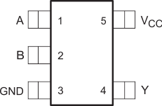
Pin Configuration and Functions

SN74AHC1G32 DBV Package5-Pin SOT-23Top View Figure 4-1 DBV Package5-Pin SOT-23Top View
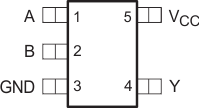
SN74AHC1G32 DCK Package5-Pin SC70Top View Figure 4-2 DCK Package5-Pin SC70Top View
SN74AHC1G32 DRL Package5-Pin SOTTop View
See mechanical drawings for dimensions.
Figure 4-3 DRL Package5-Pin SOTTop View
Table 4-1 Pin Functions
PIN TYPE(1) DESCRIPTION
NO. NAME
1 A I Input A
2 B I Input B
3 GND Ground Pin
4 Y O Output Y
5 VCC Power Pin
Signal Types: I = Input, O = Output, I/O = Input or Output