JAJSUD7C January 2003 – July 2024 CD54AC138 , CD74AC138
PRODUCTION DATA
- 1
- 1 特長
- 2 概要
- 3 Pin Configuration and Functions
-
4 Specifications
- 4.1 Absolute Maximum Ratings
- 4.2 ESD Ratings
- 4.3 Recommended Operating Conditions
- 4.4 Thermal Information
- 4.5 Electrical Characteristics
- 4.6 Switching Characteristics, VCC = 1.5V
- 4.7 Switching Characteristics, VCC = 3.3V ± 0.3V
- 4.8 Switching Characteristics, VCC = 5V ± 0.5V
- 4.9 Operating Characteristics
- 5 Parameter Measurement Information
- 6 Detailed Description
- 7 Application and Implementation
- 8 Device and Documentation Support
- 9 Revision History
- 10Mechanical, Packaging, and Orderable Information
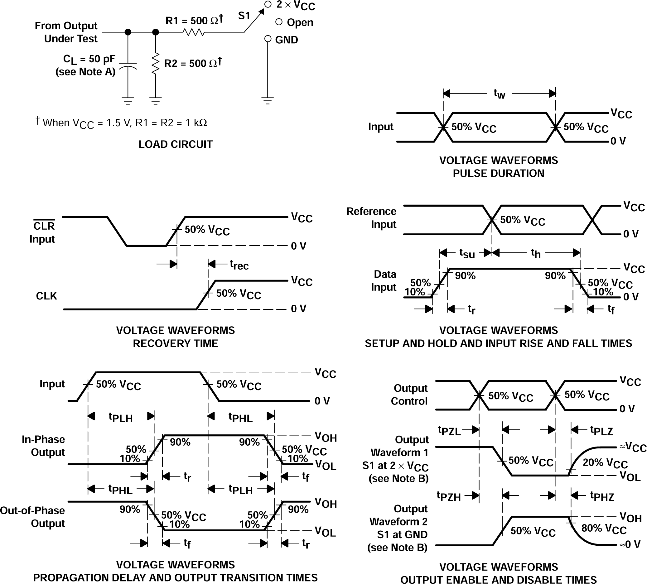
5 Parameter Measurement Information

A. CL includes probe and test-fixture capacitance.
B. Waveform 1 is for an output with internal conditions such that the output is low except when disabled by the output control. Waveform 2 is for an output with
internal conditions such that the output is high except when disabled by the output control.
C. All input pulses are supplied by generators having the following characteristics: PRR ≤ 1 MHz, ZO = 50 Ω, tr = 3 ns, tf = 3
ns. Phase relationships between waveforms are arbitrary.
D. For clock inputs, fmax is measured with the input duty cycle at 50%.
E. The outputs are measured one at a time with one input transition per measurement.
F. tPLH and tPHL are the same as tpd.
G. tPZL and tPZH are the same as ten.
H. tPLZ and tPHZ are the same as tdis.
I. All parameters and waveforms are not applicable to all devices.
Figure 5-1 Load Circuit and Voltage Waveforms| TEST | S1 |
|---|---|
| tPLH/tPHL | Open |
| tPLZ/tPZL | 2 × VCC |
| tPHZ/tPZH | GND |