JAJSUE2B April 2003 – October 2024 CD54ACT174 , CD74ACT174
PRODUCTION DATA
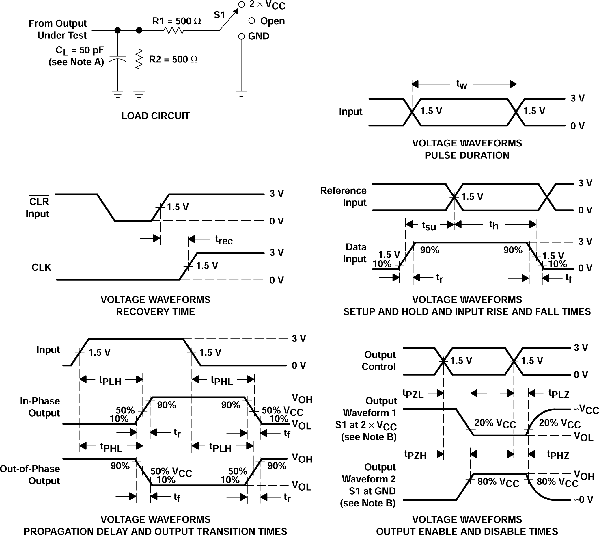
6 Parameter Measurement Information
 Figure 6-1 Load Circuit and Voltage
Waveforms
Figure 6-1 Load Circuit and Voltage
WaveformsA. CL
includes probe and test-fixture capacitance.
B. Waveform 1 is for an output
with internal conditions such that the output is low except when disabled by the
output control. Waveform 2 is for an output with internal conditions such that
the output is high except when disabled by the output control.
C. All input pulses are
supplied by generators having the following characteristics: PRR ≤ 1 MHz,
ZO = 50 Ω, tr = 3 ns, tf = 3 ns. Phase
relationships between waveforms are arbitrary.
D. For clock inputs,
fmax is measured with the input duty cycle at 50%.
E. The outputs are measured one
at a time with one input transition per measurement.
F. tPLH and
tPHL are the same as tpd.
G. tPZL and
tPZH are the same as ten.
H. tPLZ and
tPHZ are the same as tdis.
I. All parameters and waveforms
are not applicable to all devices.
| TEST | S1 |
|---|---|
| tPLH/tPHL | Open |
| tPLZ/tPZL | 2 × VCC |
| tPHZ/tPZH | GND |