JAJSUL0Q January   1993  – December 2024 SN54LVC257A , SN74LVC257A

PRODUCTION DATA  

  1.   1
  2. 特長
  3. アプリケーション
  4. 概要
  5. Pin Configuration and Functions
  6. Specifications
    1. 5.1 Absolute Maximum Ratings
    2. 5.2 ESD Ratings
    3. 5.3 Recommended Operating Conditions
    4. 5.4 Thermal Information
    5. 5.5 Electrical Characteristics
    6. 5.6 Switching Characteristics, SN54LVC257A
    7. 5.7 Switching Characteristics, SN74LVC257A
    8. 5.8 Operating Characteristics
    9. 5.9 Typical Characteristics
  7. Parameter Measurement Information
  8. Detailed Description
    1. 7.1 Overview
    2. 7.2 Functional Block Diagram
    3. 7.3 Feature Description
    4. 7.4 Device Functional Modes
  9.   Application and Implementation
    1. 8.1 Application Information
    2. 8.2 Typical Application
      1. 8.2.1 Design Requirements
      2. 8.2.2 Detailed Design Procedure
      3. 8.2.3 Application Curves
    3. 8.3 Power Supply Recommendations
    4. 8.4 Layout
      1. 8.4.1 Layout Guidelines
      2. 8.4.2 Layout Example
  10. Device and Documentation Support
    1. 8.1 Documentation Support (Analog)
      1. 8.1.1 Related Documentation
      2. 8.1.2 Related Links
    2. 8.2 Community Resources
    3. 8.3 ドキュメントの更新通知を受け取る方法
    4. 8.4 サポート・リソース
    5. 8.5 Trademarks
    6. 8.6 静電気放電に関する注意事項
    7. 8.7 用語集
  11. Revision History
  12. 10Mechanical, Packaging, and Orderable Information

Typical Characteristics

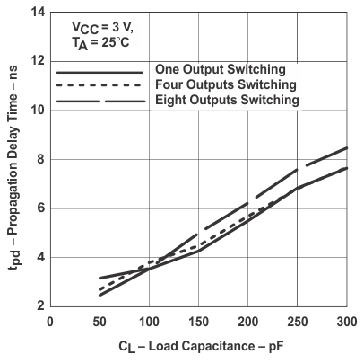
SN54LVC257A SN74LVC257A Propagation Delay (Low to High Transition) vs Load CapacitanceFigure 5-1 Propagation Delay (Low to High Transition)
vs Load Capacitance
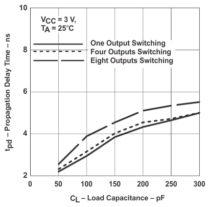
SN54LVC257A SN74LVC257A Propagation Delay (High to Low Transition) vs Load CapacitanceFigure 5-2 Propagation Delay (High to Low Transition)
vs Load Capacitance