JAJSUL9C September 2003 – May 2024 SN74LVC257A-Q1
PRODUCTION DATA
3 Pin Configuration and Functions
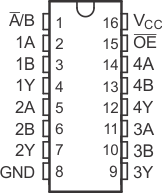
 Figure 3-1 D or PW Package,16-Pin SOIC or TSSOP(Top View)
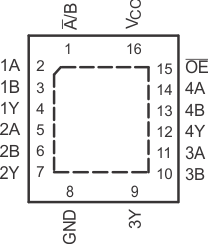
 Figure 3-2 BQB Package,16-Pin WQFN with Exposed Thermal Pad(Top View)
Table 3-1 Pin Functions
| PIN | I/O | DESCRIPTION | |
|---|---|---|---|
| NAME | SOIC, TSSOP, or WQFN | ||
| A/B | 1 | I | Select Pin, Low selects A, High selects B |
| 1A | 2 | I/O | Multiplexer Signal Input |
| 1B | 3 | I/O | Multiplexer Signal Input |
| 1Y | 4 | I/O | Multiplexer Output |
| 2A | 5 | I/O | Multiplexer Signal Input |
| 2B | 6 | I/O | Multiplexer Signal Input |
| 2Y | 7 | I/O | Multiplexer Output |
| 3A | 11 | I/O | Multiplexer Signal Input |
| 3B | 10 | I/O | Multiplexer Signal Input |
| 3Y | 9 | I/O | Multiplexer Output |
| 4A | 14 | I/O | Multiplexer Signal Input |
| 4B | 13 | I/O | Multiplexer Signal Input |
| 4Y | 12 | I/O | Multiplexer Output |
| GND | 8 | — | Ground |
| NC(1) | — | — | No connect |
| OE | 15 | I/O | Active low Output enable |
| VCC | 16 | — | Power pin |
(1) NC – no internal connection