JAJSUM1A December 1998 – May 2024 CD54AC373 , CD54ACT373 , CD74AC373 , CD74ACT373
PRODMIX
- 1
- 1 特長
- 2 概要
- 3 Pin Configuration and Functions
-
4 Specifications
- 4.1 Absolute Maximum Ratings
- 4.2 ESD Ratings
- 4.3 Recommended Operating Conditions
- 4.4 Thermal Information
- 4.5 Electrical Characteristics: AC Series
- 4.6 Electrical Characteristics: ACT Series
- 4.7 Prerequisite for Switching: AC Series
- 4.8 Switching Characteristics: AC Series
- 4.9 Prerequisite for Switching: ACT Series
- 4.10 Switching Characteristics: ACT Series
- 5 Parameter Measurement Information
- 6 Detailed Description
- 7 Application and Implementation
- 8 Device and Documentation Support
- 9 Revision History
- 10Mechanical, Packaging, and Orderable Information
3 Pin Configuration and Functions
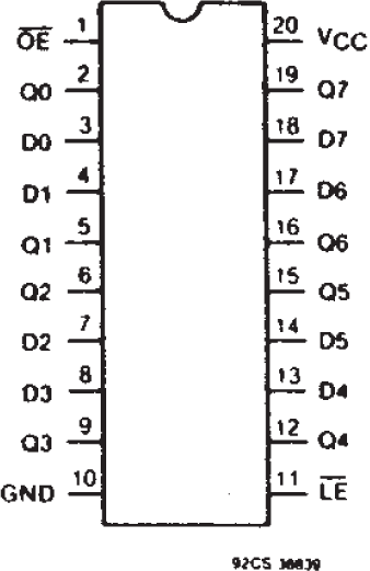
 Figure 3-1 CDx4AC373, CDx4ACT373
| PIN | I/O | DESCRIPTION | |
|---|---|---|---|
| NAME | NO. | ||
| OE | 1 | Input | 3-state output enable input |
| 0Q | 2 | Output | Output for channel 0 |
| 0D | 3 | Input | Input for channel 0 |
| 1D | 4 | Input | Input for channel 1 |
| 1Q | 5 | Output | Output for channel 1 |
| 2Q | 6 | Output | Output for channel 2 |
| 2D | 7 | Input | Input for channel 2 |
| 3D | 8 | Input | Input for channel 3 |
| 3Q | 9 | Output | Output for channel 3 |
| GND | 10 | — | Ground |
| LE | 11 | Input | Latch enable input (active HIGH) |
| 4Q | 12 | Output | Output for channel 4 |
| 4D | 13 | Input | Input for channel 4 |
| 5D | 14 | Input | Input for channel 5 |
| 5Q | 15 | Output | Output for channel 5 |
| 6Q | 16 | Output | Output for channel 6 |
| 6D | 17 | Input | Input for channel 6 |
| 7D | 18 | Input | Input for channel 7 |
| 7Q | 19 | Output | Output for channel 7 |
| VCC | 20 | — | Supply voltage |