JAJSUR6D January 2004 – June 2024 SN74HC4851-Q1
PRODUCTION DATA
6 Parameter Measurement Information
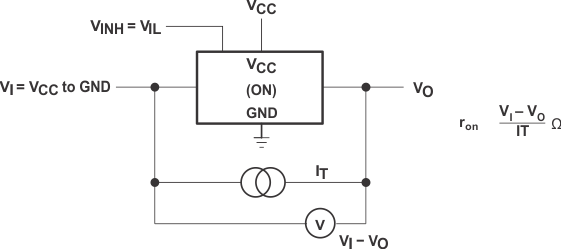 Figure 6-1 On-State-Resistance Test Circuit
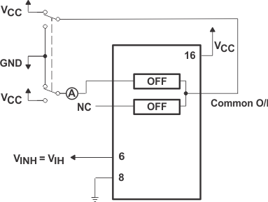 Figure 6-2 Maximum Off-Channel Leakage Current, Any One Channel, Test Setup
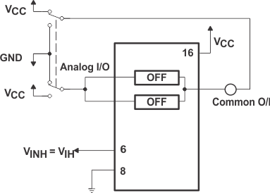 Figure 6-3 Maximum Off-Channel Leakage Current, Common Channel, Test Setup
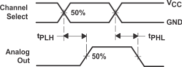 Figure 6-5 Propagation Delays, Channel Select to Analog Out
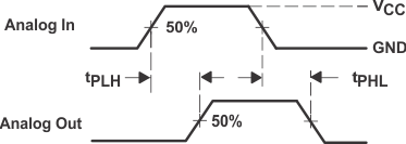 Figure 6-7 Propagation Delays, Analog In to Analog Out
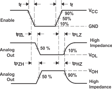 Figure 6-9 Propagation Delays, Enable to Analog Out
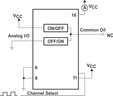 Figure 6-11 Power-Dissipation Capacitance Test Setup
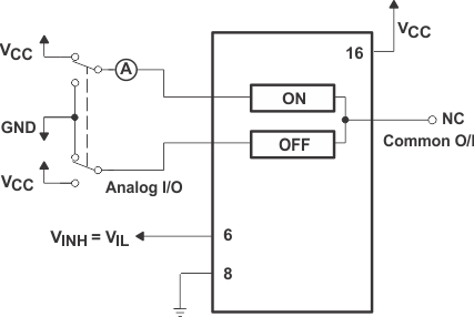 Figure 6-4 Maximum On-Channel Leakage Current, Channel To Channel, Test Setup
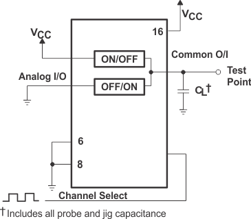 Figure 6-6 Propagation-Delay Test Setup, Channel Select to Analog Out
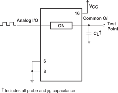 Figure 6-8 Propagation-Delay Test Setup, Analog In to Analog Out
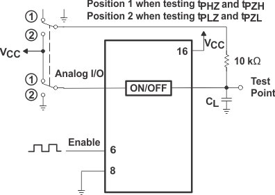 Figure 6-10 Propagation-Delay Test Setup, Enable to Analog Out