JAJSUR7C September 2003 – June 2024 SN74HC4851
PRODUCTION DATA
8.1 Application Information
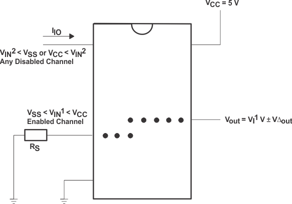
 Figure 8-1 Injection-Current Coupling Specification
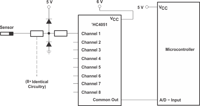
 Figure 8-2 Alternate
Solution Requires 32 Passive Components and One Extra 6-V Regulator to Suppress
Injection Current Into a Standard ’HC4051 Multiplexer
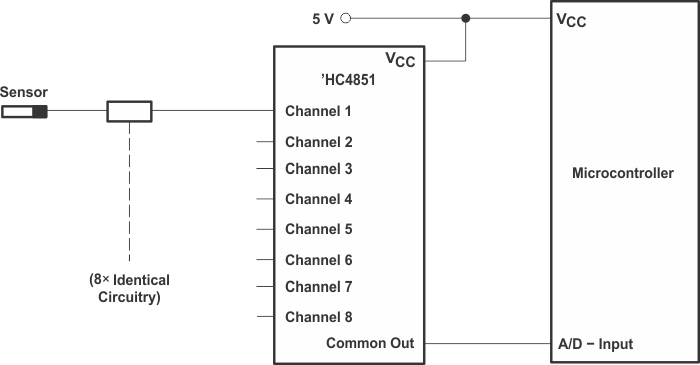
 Figure 8-3 Solution
by Applying the ’HC4851 Multiplexer
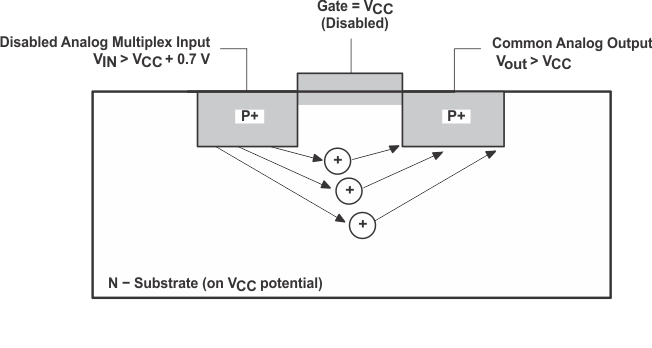
 Figure 8-4 Diagram
of Bipolar Coupling Mechanism (Appears if VIN Exceeds VCC,
Driving Injection Current Into the Substrate)