JAJSUR8B December 2006 – June 2024 SN74HC4852-Q1
PRODUCTION DATA
8.1 Application Information
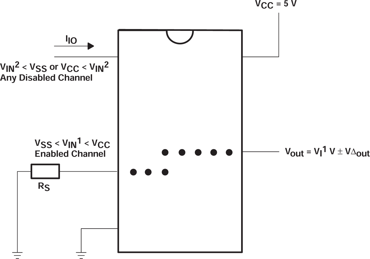
 Figure 8-1 Injection-Current Coupling Specification
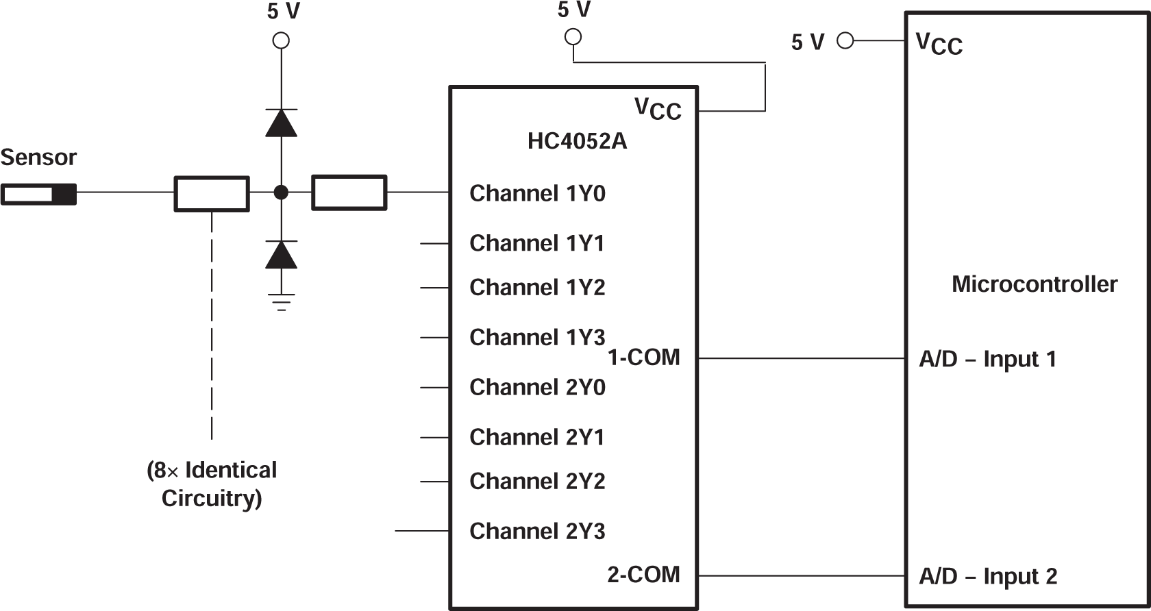
 Figure 8-2 Actual Technology Requires 32 Passive Components and One Extra 6-v Regulator to Suppress Injection Current into a Standard HC4052 Multiplexer
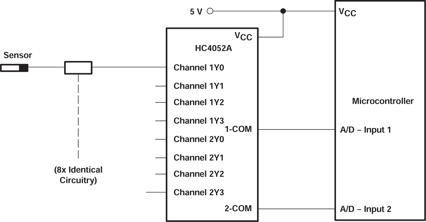
 Figure 8-3 Solution by Applying the HC4852 Multiplexer
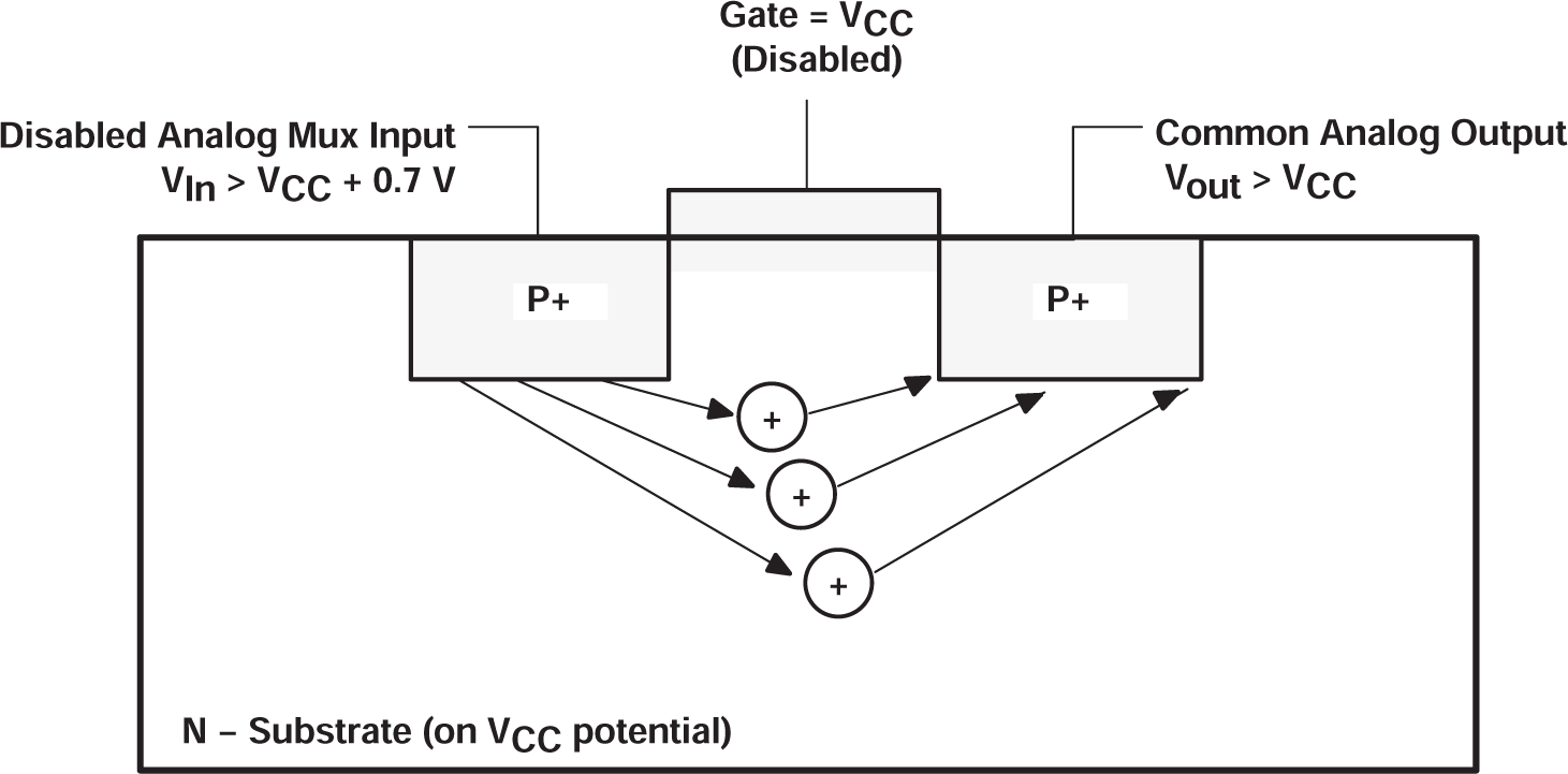
 Figure 8-4 Diagram of Bipolar Coupling Mechanism (Appears If VIn Exceeds VCC, Driving Injection Current into the Substrate)