JAJSUR9A March   2004  – June 2024 SN74HC4852

PRODUCTION DATA  

  1.   1
  2. 特長
  3. アプリケーション
  4. 概要
  5. Pin Configuration and Functions
  6. Specifications
    1. 5.1 Absolute Maximum Ratings
    2. 5.2 ESD Ratings
    3. 5.3 Thermal Information: SN74HC485x
    4. 5.4 Recommended Operating Conditions
    5. 5.5 Electrical Characteristics
    6. 5.6 Timing Characteristics
    7. 5.7 Injection Current Coupling
  7. Parameter Measurement Information
  8. Detailed Description
    1. 7.1 Functional Block Diagram
  9. Application and Implementation
    1. 8.1 Application Information
  10. Device and Documentation Support
    1. 9.1 ドキュメントの更新通知を受け取る方法
    2. 9.2 サポート・リソース
    3. 9.3 Trademarks
    4. 9.4 静電気放電に関する注意事項
    5. 9.5 用語集
  11. 10Revision History
  12. 11Mechanical, Packaging, and Orderable Information

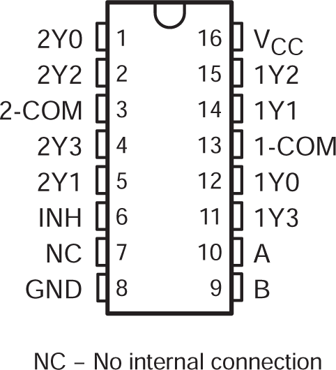
Pin Configuration and Functions

SN74HC4852 PW Package, 16-Pin TSSOP (Top
          View) Figure 4-1 PW Package, 16-Pin TSSOP (Top View)
Table 4-1 Function Table
INPUTS ON CHANNEL
INH B A
L L L 1Y0, 2Y0
L L H 1Y1, 2Y1
L H L 1Y2, 2Y2
L H H 1Y3, 2Y3
H X X None