JAJSUT1B June 2024 – November 2024 TUSB2E221
PRODMIX
- 1
- 1 特長
- 2 アプリケーション
- 3 概要
- 4 Device Variants
- 5 Pin Configuration and Functions
- 6 Specifications
- 7 Parametric Measurement Information
-
8 Detailed Description
- 8.1 Overview
- 8.2 Functional Block Diagram
- 8.3 Feature Description
- 8.4 Device Functional Modes
- 8.5 Programming
- 9 Register Map
- 10Applications and Implementation
- 11Device and Documentation Support
- 12Revision History
- 13Mechanical, Packaging, and Orderable Information
10.4.1 Layout Guidelines
- Place supply bypass capacitors as close to VDD1V8 and VDD3V3 pins as possible and avoid placing the bypass caps near the eDP/eDN and DP/DN traces.
- Route the high-speed USB signals using a minimum of vias and corners which reduces signal reflections and impedance changes. When a via must be used, increase the clearance size around the via to minimize the capacitance. Each via introduces discontinuities in the transmission line of the signal and increases the chance of picking up interference from the other layers of the board. Be careful when designing test points on twisted pair lines; through-hole pins are not recommended.
- When it becomes necessary to turn 90°, use two 45° turns or an arc instead of making a single 90° turn. This reduces reflections on the signal traces by minimizing impedance discontinuities.
- Do not route USB traces under or near crystals, oscillators, clock signal generators, switching regulators, mounting holes, magnetic devices or ICs that use or duplicate clock signals.
- Avoid stubs on the high-speed USB signals due to signal reflections. If a stub is unavoidable, then the stub must be less than 200 mil
- Route all high-speed USB signal traces over continuous GND planes, with no interruptions.
- Avoid crossing over anti-etch, commonly found with plane splits.
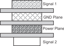
- Due to high frequencies associated with the USB, a printed circuit board with at least four layers is recommended; two signal layers separated by a ground and power layer as shown in Figure 10-3.
 Figure 10-3 Four-Layer Board Stack-Up