JAJSUU0 June 2024 TXS0104V
PRODUCTION DATA
- 1
- 1 特長
- 2 アプリケーション
- 3 概要
- 4 Pin Configuration and Functions
-
5 Specifications
- 5.1 Absolute Maximum Ratings
- 5.2 ESD Ratings
- 5.3 Recommended Operating Conditions
- 5.4 Thermal Information (PW, RGY, BQA, RUT, D)
- 5.5 Electrical Characteristics
- 5.6 Switching Characteristics, VCCA = 1.8 ± 0.15V
- 5.7 Switching Characteristics, VCCA = 2.5 ± 0.2V
- 5.8 Switching Characteristics, VCCA = 3.3 ± 0.3V
- 5.9 Switching Characteristics: Tsk, TMAX
- 5.10 Typical Characteristics
- 6 Parameter Measurement Information
- 7 Detailed Description
- 8 Application and Implementation
- 9 Device and Documentation Support
- 10Revision History
- 11Mechanical, Packaging, and Orderable Information
6.2 Voltage Waveforms
The outputs are measured one at a time, with one transition per measurement. All input pulses are supplied by generators that have the following characteristics:
- PRR ≤ 10MHz
- ZO = 50Ω
- dv/dt ≥ 1V/ns
 Figure 6-4 Pulse Duration
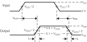
 Figure 6-5 Propagation Delay Times
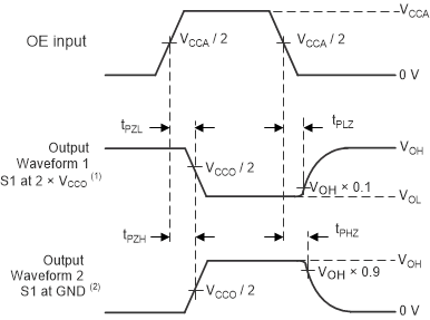
A. Waveform 1 is for an output with internal such that the output is high, except when OE is high (see Figure 6-3).
B. Waveform 2 is for an output with conditions such that the output is low, except when OE is high.
Figure 6-6 Enable and Disable Times