JAJSUV6C November 2008 – October 2024 TS3USB221A
PRODUCTION DATA
- 1
- 1 特長
- 2 アプリケーション
- 3 概要
- 4 Pin Configuration and Functions
-
5 Specifications
- 5.1 Absolute Maximum Ratings
- 5.2 ESD Ratings
- 5.3 Recommended Operating Conditions
- 5.4 Thermal Information
- 5.5 Electrical Characteristics
- 5.6 Dynamic Electrical Characteristics, VCC = 3.3V ±10%
- 5.7 Dynamic Electrical Characteristics, VCC = 2.5V ±10%
- 5.8 Switching Characteristics, VCC = 3.3V ±10%
- 5.9 Switching Characteristics, VCC = 2.5V ±10%
- 5.10 Typical Characteristics
- 6 Parameter Measurement Information
- 7 Detailed Description
- 8 Application and Implementation
- 9 Device and Documentation Support
- 10Revision History
- 11Mechanical, Packaging, and Orderable Information
8.2.3 Application Curves
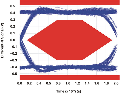
 Figure 8-2 Eye Pattern: 480Mbps USB Signal With No Switch (Through Path)
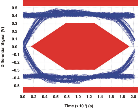
 Figure 8-4 Eye Pattern: 480Mbps USB Signal With Switch NO Path
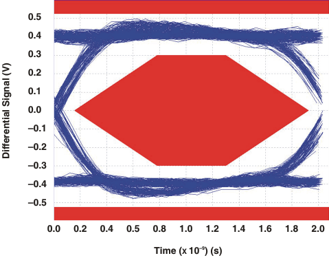
 Figure 8-3 Eye Pattern: 480Mbps USB Signal With Switch NC Path