JAJSUX5 June 2024 TMUX1308A-Q1 , TMUX1309A-Q1
PRODUCTION DATA
- 1
- 1 特長
- 2 アプリケーション
- 3 概要
- 4 Device Comparison Table
- 5 Pin Configuration and Functions
-
6 Specifications
- 6.1 Absolute Maximum Ratings
- 6.2 ESD Ratings
- 6.3 Thermal Information: TMUX1308A-Q1
- 6.4 Thermal Information: TMUX1309A-Q1
- 6.5 Recommended Operating Conditions
- 6.6 Electrical Characteristics
- 6.7 Logic and Dynamic Characteristics
- 6.8 Timing Characteristics
- 6.9 Injection Current Coupling
- 6.10 Typical Characteristics
- 7 Parameter Measurement Information
-
8 Detailed Description
- 8.1 Overview
- 8.2 Functional Block Diagram
- 8.3
Feature Description
- 8.3.1 Bidirectional Operation
- 8.3.2 Rail-to-Rail Operation
- 8.3.3 1.8V Logic Compatible Inputs
- 8.3.4 Fail-Safe Logic
- 8.3.5 High-Impedance Optimization
- 8.3.6
Injection Current Control
- 8.3.6.1 TMUX13xxA-Q1 is Powered, Channel is Unselected, and the Input Signal is Greater Than VDD (VDD = 5V, VINPUT = 5.5V)
- 8.3.6.2 TMUX13xxA-Q1 is Powered, Channel is Selected, and the Input Signal is Greater Than VDD (VDD = 5V, VINPUT = 5.5V)
- 8.3.6.3 TMUX13xxA-Q1 is Unpowered and the Input Signal has a Voltage Present (VDD = 0V, VINPUT = 3V)
- 8.4 Device Functional Modes
- 8.5 Truth Tables
- 9 Application and Implementation
- 10Device and Documentation Support
- 11Mechanical, Packaging, and Orderable Information
- 12Revision History
7.1 On-Resistance
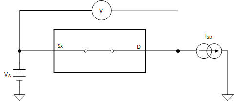
The on-resistance of a device is the ohmic resistance between the source (Sx) and drain (D) pins of the device. The on-resistance varies with input voltage and supply voltage. The symbol RON is used to denote on-resistance. The measurement setup used to measure RON is shown in the following figure. Voltage (V) and current (ISD) are measured using this setup, and RON is computed as shown in Figure 7-1 with RON = V / ISD:
 Figure 7-1 On-Resistance Measurement Setup