JAJSUY7 May   2024 MCT8316A-Q1

PRODUCTION DATA  

  1.   1
  2. 特長
  3. アプリケーション
  4. 概要
  5. Pin Configuration and Functions
  6. Specifications
    1. 5.1 Absolute Maximum Ratings
    2. 5.2 ESD Ratings Auto
    3. 5.3 Recommended Operating Conditions
    4. 5.4 Thermal Information
    5. 5.5 Electrical Characteristics
    6. 5.6 Characteristics of the SDA and SCL bus for Standard and Fast mode
  7. Detailed Description
    1. 6.1 Overview
    2. 6.2 Functional Block Diagram
    3. 6.3 Feature Description
      1. 6.3.1  Output Stage
      2. 6.3.2  Device Interface Modes
        1. 6.3.2.1 Interface - Control and Monitoring
        2. 6.3.2.2 I2C Interface
      3. 6.3.3  Step-Down Mixed-Mode Buck Regulator
        1. 6.3.3.1 Buck in Inductor Mode
        2. 6.3.3.2 Buck in Resistor mode
        3. 6.3.3.3 Buck Regulator with External LDO
        4. 6.3.3.4 AVDD Power Sequencing from Buck Regulator
        5. 6.3.3.5 Mixed Mode Buck Operation and Control
        6. 6.3.3.6 Buck Undervoltage Protection
        7. 6.3.3.7 Buck Overcurrent Protection
      4. 6.3.4  AVDD Linear Voltage Regulator
      5. 6.3.5  Charge Pump
      6. 6.3.6  Slew Rate Control
      7. 6.3.7  Cross Conduction (Dead Time)
      8. 6.3.8  SPEED Control
        1. 6.3.8.1 Analog-Mode Speed Control
        2. 6.3.8.2 PWM-Mode Speed Control
        3. 6.3.8.3 I2C based Speed Control
        4. 6.3.8.4 Frequency-Mode Speed Control
      9. 6.3.9  Starting the Motor Under Different Initial Conditions
        1. 6.3.9.1 Case 1 – Motor is Stationary
        2. 6.3.9.2 Case 2 – Motor is Spinning in the Forward Direction
        3. 6.3.9.3 Case 3 – Motor is Spinning in the Reverse Direction
      10. 6.3.10 Motor Start Sequence (MSS)
        1. 6.3.10.1 Initial Speed Detect (ISD)
        2. 6.3.10.2 Motor Resynchronization
        3. 6.3.10.3 Reverse Drive
        4. 6.3.10.4 Motor Start-up
          1. 6.3.10.4.1 Align
          2. 6.3.10.4.2 Double Align
          3. 6.3.10.4.3 Initial Position Detection (IPD)
            1. 6.3.10.4.3.1 IPD Operation
            2. 6.3.10.4.3.2 IPD Release Mode
            3. 6.3.10.4.3.3 IPD Advance Angle
          4. 6.3.10.4.4 Slow First Cycle Startup
          5. 6.3.10.4.5 Open loop
          6. 6.3.10.4.6 Transition from Open to Closed Loop
      11. 6.3.11 Closed Loop Operation
        1. 6.3.11.1 120o Commutation
          1. 6.3.11.1.1 High-Side Modulation
          2. 6.3.11.1.2 Low-Side Modulation
          3. 6.3.11.1.3 Mixed Modulation
        2. 6.3.11.2 Variable Commutation
        3. 6.3.11.3 Lead Angle Control
        4. 6.3.11.4 Closed loop accelerate
      12. 6.3.12 Speed Loop
      13. 6.3.13 Input Power Regulation
      14. 6.3.14 Anti-Voltage Surge (AVS)
      15. 6.3.15 Output PWM Switching Frequency
      16. 6.3.16 Fast Start-up (< 50 ms)
        1. 6.3.16.1 BEMF Threshold
        2. 6.3.16.2 Dynamic Degauss
      17. 6.3.17 Fast Deceleration
      18. 6.3.18 Active Demagnetization
        1. 6.3.18.1 Active Demagnetization in action
      19. 6.3.19 Motor Stop Options
        1. 6.3.19.1 Coast (Hi-Z) Mode
        2. 6.3.19.2 Recirculation Mode
        3. 6.3.19.3 Low-Side Braking
        4. 6.3.19.4 High-Side Braking
        5. 6.3.19.5 Active Spin-Down
      20. 6.3.20 FG Configuration
        1. 6.3.20.1 FG Output Frequency
        2. 6.3.20.2 FG Open-Loop and Lock Behavior
      21. 6.3.21 Protections
        1. 6.3.21.1  VM Supply Undervoltage Lockout
        2. 6.3.21.2  AVDD Undervoltage Lockout (AVDD_UV)
        3. 6.3.21.3  BUCK Undervoltage Lockout (BUCK_UV)
        4. 6.3.21.4  VCP Charge Pump Undervoltage Lockout (CPUV)
        5. 6.3.21.5  Overvoltage Protection (OVP)
        6. 6.3.21.6  Overcurrent Protection (OCP)
          1. 6.3.21.6.1 OCP Latched Shutdown (OCP_MODE = 00b)
          2. 6.3.21.6.2 OCP Automatic Retry (OCP_MODE = 01b)
          3. 6.3.21.6.3 OCP Report Only (OCP_MODE = 10b)
          4. 6.3.21.6.4 OCP Disabled (OCP_MODE = 11b)
        7. 6.3.21.7  Buck Overcurrent Protection
        8. 6.3.21.8  Cycle-by-Cycle (CBC) Current Limit (CBC_ILIMIT)
          1. 6.3.21.8.1 CBC_ILIMIT Automatic Recovery next PWM Cycle (CBC_ILIMIT_MODE = 000xb)
          2. 6.3.21.8.2 CBC_ILIMIT Automatic Recovery Threshold Based (CBC_ILIMIT_MODE = 001xb)
          3. 6.3.21.8.3 CBC_ILIMIT Automatic Recovery after 'n' PWM Cycles (CBC_ILIMIT_MODE = 010xb)
          4. 6.3.21.8.4 CBC_ILIMIT Report Only (CBC_ILIMIT_MODE = 0110b)
          5. 6.3.21.8.5 CBC_ILIMIT Disabled (CBC_ILIMIT_MODE = 0111b or 1xxxb)
        9. 6.3.21.9  Lock Detection Current Limit (LOCK_ILIMIT)
          1. 6.3.21.9.1 LOCK_ILIMIT Latched Shutdown (LOCK_ILIMIT_MODE = 00xxb)
          2. 6.3.21.9.2 LOCK_ILIMIT Automatic Recovery (LOCK_ILIMIT_MODE = 01xxb)
          3. 6.3.21.9.3 LOCK_ILIMIT Report Only (LOCK_ILIMIT_MODE = 1000b)
          4. 6.3.21.9.4 LOCK_ILIMIT Disabled (LOCK_ILIMIT_MODE = 1xx1b)
        10. 6.3.21.10 Thermal Warning (OTW)
        11. 6.3.21.11 Thermal Shutdown (TSD)
        12. 6.3.21.12 Motor Lock (MTR_LCK)
          1. 6.3.21.12.1 MTR_LCK Latched Shutdown (MTR_LCK_MODE = 00xxb)
          2. 6.3.21.12.2 MTR_LCK Automatic Recovery (MTR_LCK_MODE= 01xxb)
          3. 6.3.21.12.3 MTR_LCK Report Only (MTR_LCK_MODE = 1000b)
          4. 6.3.21.12.4 MTR_LCK Disabled (MTR_LCK_MODE = 1xx1b)
        13. 6.3.21.13 Motor Lock Detection
          1. 6.3.21.13.1 Lock 1: Abnormal Speed (ABN_SPEED)
          2. 6.3.21.13.2 Lock 2: Loss of Sync (LOSS_OF_SYNC)
          3. 6.3.21.13.3 Lock3: No-Motor Fault (NO_MTR)
        14. 6.3.21.14 IPD Faults
    4. 6.4 Device Functional Modes
      1. 6.4.1 Functional Modes
        1. 6.4.1.1 Sleep Mode
        2. 6.4.1.2 Standby Mode
        3. 6.4.1.3 Fault Reset (CLR_FLT)
    5. 6.5 External Interface
      1. 6.5.1 DRVOFF Functionality
      2. 6.5.2 DAC outputs
      3. 6.5.3 SOX Output
      4. 6.5.4 Oscillator Source
        1. 6.5.4.1 External Clock Source
      5. 6.5.5 External Watchdog
    6. 6.6 EEPROM access and I2C interface
      1. 6.6.1 EEPROM Access
        1. 6.6.1.1 EEPROM Write
        2. 6.6.1.2 EEPROM Read
      2. 6.6.2 I2C Serial Interface
        1. 6.6.2.1 I2C Data Word
        2. 6.6.2.2 I2C Write Operation
        3. 6.6.2.3 I2C Read Operation
        4. 6.6.2.4 Examples of MCT8316A-Q1 I2C Communication Protocol Packets
        5. 6.6.2.5 Internal Buffers
        6. 6.6.2.6 CRC Byte Calculation
    7. 6.7 EEPROM (Non-Volatile) Register Map
      1. 6.7.1 Algorithm_Configuration Registers
      2. 6.7.2 Fault_Configuration Registers
      3. 6.7.3 Hardware_Configuration Registers
      4. 6.7.4 Gate_Driver_Configuration Registers
    8. 6.8 RAM (Volatile) Register Map
      1. 6.8.1 Fault_Status Registers
      2. 6.8.2 System_Status Registers
      3. 6.8.3 Algo_Control Registers
      4. 6.8.4 Device_Control Registers
  8. Application and Implementation
    1. 7.1 Application Information
    2. 7.2 Typical Applications
      1. 7.2.1 Application Curves
        1. 7.2.1.1 Motor startup
        2. 7.2.1.2 120o and variable commutation
        3. 7.2.1.3 Faster startup time
        4. 7.2.1.4 Setting the BEMF threshold
        5. 7.2.1.5 Maximum speed
        6. 7.2.1.6 Faster deceleration
    3. 7.3 Power Supply Recommendations
      1. 7.3.1 Bulk Capacitance
    4. 7.4 Layout
      1. 7.4.1 Layout Guidelines
      2. 7.4.2 Layout Example
      3. 7.4.3 Thermal Considerations
        1. 7.4.3.1 Power Dissipation
  9. Device and Documentation Support
    1. 8.1 サポート・リソース
    2. 8.2 Trademarks
    3. 8.3 静電気放電に関する注意事項
    4. 8.4 用語集
  10. Revision History
  11. 10Mechanical, Packaging, and Orderable Information

Setting the BEMF threshold

The BEMF_THRESHOLD1 and BEMF_THRESHOLD2 values used for commutation instant detection in MCT8316A can be computed from the motor phase voltage waveforms during coasting. For example, consider the three-phase voltage waveforms of a BLDC motor while coasting as in Figure 7-6. The motor phase voltage during coasting is the motor back-EMF.
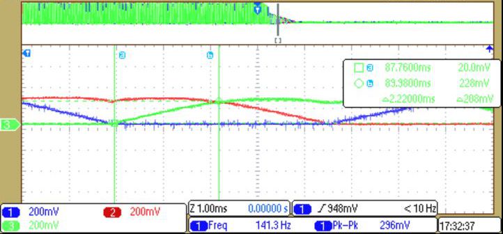
MCT8316A-Q1 Motor phase voltage during coasting Figure 7-6 Motor phase voltage during coasting

In Figure 7-6, one floating phase voltage interval is denoted by the vertical markers on channel 3. The Vpeak (peak-peak back-EMF) on channel 3 is 208mV and Tc (commutation interval) is 2.22ms as denoted by the horizontal and vertical markers on channel 3. The digital equivalent counts for Vpeak and Tc are calculated as follows.

In MCT8316A, a 3V analog input corresponds to 4095 counts(12-bit) and phase voltage is scaled down by 10x factor before ADC input; therfore, Vpeak of 208mV corresponds to an ADC input of 20.8mV, which in turn equals 29 ADC counts. Assuming the PWM switching frequency is 25kHz, one back-EMF sample is available every 40μs. So, in a time interval of 2.22ms, a total of 55 back-EMF samples are integrated. Therefore, the BEMF_THRESHOLD1 or BEMF_THRESHOLD2 value calculated as per is (½) * (29/2) * (55/2) = 199. Hence, in this example, BEMF_THRESHOLD1 and BEMF_THRESHOLD2 are set to 8h (corresponding to 200 which is the closest value to 199) for commutation instant detection using back-EMF integration method during fast start-up. The exact speed at which the Vpeak and Tc values are measured to calculate the BEMF_THRESHOLD1 and BEMF_THRESHOLD2 values is not critical (as long as there is sufficient resolution in digital counts) since the product (Vpeak * Tc) is, largely, a constant for a given BLDC motor.