JAJSV29D August   1995  – July 2024 SN54ACT86 , SN74ACT86

PRODUCTION DATA  
  1.   1
  2. 特長
  3. 概要
  4. Pin Configuration and Functions
  5. Specifications
    1. 4.1 Absolute Maximum Ratings
    2. 4.2 Recommended Operating Conditions
    3. 4.3 Thermal Information
    4. 4.4 Electrical Characteristics
    5. 4.5 Switching Characteristics
    6. 4.6 Operating Characteristics
  6. Parameter Measurement Information
  7. Detailed Description
    1. 6.1 Functional Block Diagram
    2. 6.2 Device Functional Modes
  8. Application and Implementation
    1. 7.1 Power Supply Recommendations
    2. 7.2 Layout
      1. 7.2.1 Layout Guidelines
      2. 7.2.2 Layout Example
  9. Device and Documentation Support
    1. 8.1 Documentation Support
      1. 8.1.1 Related Links
    2. 8.2 ドキュメントの更新通知を受け取る方法
    3. 8.3 サポート・リソース
    4. 8.4 Trademarks
    5. 8.5 静電気放電に関する注意事項
    6. 8.6 用語集
  10. Revision History
  11. 10Mechanical, Packaging, and Orderable Information

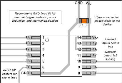
Layout Example

SN54ACT86 SN74ACT86 Example
                    layout for the SN74ACT86 
                Figure 7-1 Example layout for the SN74ACT86