JAJSV55 August 2024 BQ2969
PRODUCTION DATA
- 1
- 1 特長
- 2 アプリケーション
- 3 概要
- 4 Device Comparison Table
- 5 Pin Configuration and Functions
- 6 Specifications
- 7 Detailed Description
- 8 Application and Implementation
- 9 Power Supply Recommendations
- 10Layout
- 11Device and Documentation Support
- 12Revision History
- 13Mechanical, Packaging, and Orderable Information
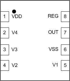
5 Pin Configuration and Functions
 Figure 5-1 2-Series to 4-Series BQ2969 (Top
View)
Figure 5-1 2-Series to 4-Series BQ2969 (Top
View)Table 5-1 Pin Functions
| PIN | TYPE(1) | DESCRIPTION | ||
|---|---|---|---|---|
| NAME | BQ2962 | |||
| VDD | 1 | P | Power supply input | |
| V4 | 2 | IA | Sense input for positive voltage of the fourth cell from the bottom of the stack | |
| V3 | 3 | IA | Sense input for positive voltage of the third cell from the bottom of the stack | |
| V2 | 4 | IA | Sense input for positive voltage of the second cell from the bottom of the stack | |
| V1 | 5 | IA | Sense input for positive voltage of the lowest cell from the bottom of the stack | |
| VSS | 6 | P | Electrically connected to integrated circuit ground and negative terminal of the lowest cell in the stack | |
| OUT | 7 | OA | Analog output drive for an overvoltage fault signal; CMOS output high or open-drain active pulldown or open-drain inactive pulldown | |
| REG | 8 | OA | Regulated supply output. Requires an external ceramic capacitor for stability | |
| PWPD | - | P | TI recommends connecting the exposed pad to VSS on PCB. | |
(1) IA = Analog input, OA = Analog
Output, P = Power connection