JAJSV93Q
October 1995 – August 2024
SN54AHCT541
,
SN74AHCT541
PRODUCTION DATA
1
1
特長
2
概要
3
Pin Configuration and Functions
4
Specifications
4.1
Absolute Maximum Ratings
4.2
ESD Ratings
4.3
Recommended Operating Conditions
4.4
Thermal Information
4.5
Electrical Characteristics
4.6
Switching Characteristics
4.7
Operating Characteristics
5
Parameter Measurement Information
6
Detailed Description
6.1
Overview
6.2
Functional Block Diagram
6.3
Device Functional Modes
7
Application and Implementation
7.1
Power Supply Recommendations
7.2
Layout
7.2.1
Layout Guidelines
7.2.2
Layout Example
8
Device and Documentation Support
8.1
Device and Documentation Support
8.1.1
Related Links
8.2
ドキュメントの更新通知を受け取る方法
8.3
サポート・リソース
8.4
Trademarks
8.5
静電気放電に関する注意事項
8.6
Glossary
9
Revision History
10
Mechanical, Packaging, and Orderable Information
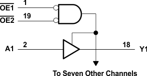
6.2
Functional Block Diagram