JAJSV94N December   1995  – August 2024 SN54AHCT540 , SN74AHCT540

PRODUCTION DATA  

  1.   1
  2. 特長
  3. 概要
  4. Pin Configuration and Functions
  5. Specifications
    1. 4.1 Absolute Maximum Ratings
    2. 4.2 ESD Ratings
    3. 4.3 Recommended Operating Conditions
    4. 4.4 Thermal Information
    5. 4.5 Electrical Characteristics
    6. 4.6 Switching Characteristics
    7. 4.7 Operating Characteristics
  6. Parameter Measurement Information
  7. Detailed Description
    1. 6.1 Overview
    2. 6.2 Functional Block Diagram
    3. 6.3 Device Functional Modes
  8. Application and Implementation
    1. 7.1 Power Supply Recommendations
    2. 7.2 Layout
      1. 7.2.1 Layout Guidelines
      2. 7.2.2 Layout Example
  9. Device and Documentation Support
    1. 8.1 Documentation Support (Analog)
      1. 8.1.1 Related Links
    2. 8.2 ドキュメントの更新通知を受け取る方法
    3. 8.3 サポート・リソース
    4. 8.4 Trademarks
    5. 8.5 静電気放電に関する注意事項
    6. 8.6 用語集
  10. Revision History
  11. 10Mechanical, Packaging, and Orderable Information

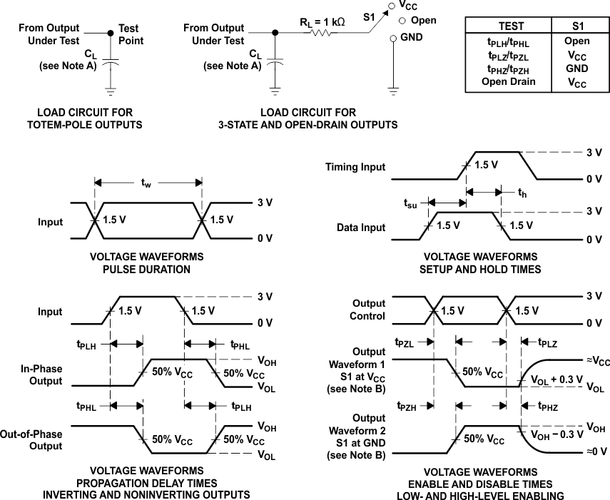
Parameter Measurement Information

SN74AHCT540 SN54AHCT540 Load
                    Circuit and Voltage Waveforms
CL includes probe and jig capacitance.
Waveform 1 is for an output with internal conditions such that the output is low except when disabled by the output control.
Waveform 2 is for an output with internal conditions such that the output is high except when disabled by the output control.
All input pulses are supplied by generators having the following characteristics: PRR ≤ 1 MHz, ZO = 50 Ω, tr ≤ 3 ns, tf ≤ 3 ns.
The outputs are measured one at a time with one input transition per measurement.
All parameters and waveforms are not applicable to all devices.
Figure 5-1 Load Circuit and Voltage Waveforms