JAJSVE5 September 2024 DDS39RF12 , DDS39RFS12
PRODUCTION DATA
- 1
- 1 特長
- 2 アプリケーション
- 3 概要
- 4 Device Comparison
- 5 Pin Configuration and Functions
-
6 Specifications
- 6.1 Absolute Maximum Ratings
- 6.2 ESD Ratings
- 6.3 Recommended Operating Conditions
- 6.4 Thermal Information
- 6.5 Electrical Characteristics - DC Specifications
- 6.6 Electrical Characteristics - AC Specifications
- 6.7 Electrical Characteristics - Power Consumption
- 6.8 Timing Requirements
- 6.9 Switching Characteristics
- 6.10 SPI and FRI Timing Diagrams
- 6.11 Typical Characteristics: Single Tone Spectra
- 6.12 Typical Characteristics: Dual Tone Spectra
- 6.13 Typical Characteristics: Power Dissipation and Supply Currents
-
7 Detailed Description
- 7.1 Overview
- 7.2 Functional Block Diagrams
- 7.3
Feature Description
- 7.3.1 DAC Output Modes
- 7.3.2 DAC Core
- 7.3.3 DEM and Dither
- 7.3.4 Offset Adjustment
- 7.3.5 Clocking Subsystem
- 7.3.6 Digital Signal Processing Blocks
- 7.3.7
JESD204C Interface
- 7.3.7.1 Deviation from JESD204C Standard
- 7.3.7.2 Transport Layer
- 7.3.7.3 Scrambler and Descrambler
- 7.3.7.4 Link Layer
- 7.3.7.5 Physical Layer
- 7.3.7.6 Serdes PLL Control
- 7.3.7.7 Serdes Crossbar
- 7.3.7.8 Multi-Device Synchronization and Deterministic Latency
- 7.3.7.9 Operation in Subclass 0 Systems
- 7.3.7.10 Link Reset
- 7.3.8 Alarm Generation
- 7.4 Device Functional Modes
- 7.5 Programming
- 8 Application and Implementation
- 9 Device and Documentation Support
- 10Revision History
- 11Mechanical, Packaging, and Orderable Information
7.3.7.8 Multi-Device Synchronization and Deterministic Latency
JESD204C subclass 1 outlines a method to achieve deterministic latency across the serial link. If two devices achieve the same deterministic latency then the devices are considered synchronized. This latency must be achieved from system startup to startup to be deterministic. There are two key requirements to achieve deterministic latency. The first is proper capture of SYSREF. SYSREF resets the LMFC counter in each device to act as a known timing reference.
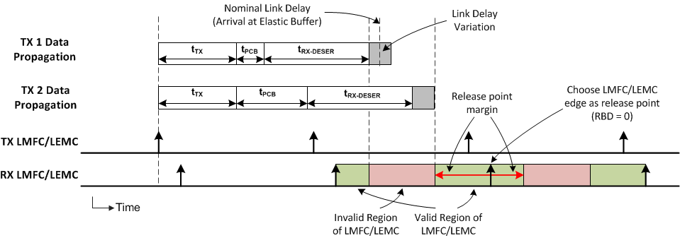
The second requirement is to choose a proper elastic buffer release point in the receiver. The converter device is the receiver (RX) in the JESD204C link and the logic device is the transmitter (TX). The elastic buffer is the key block for achieving deterministic latency and does so by absorbing variations in the propagation delays of the serialized data as the data travels from the transmitter to the receiver. A proper release point is one that provides sufficient margin against delay variations. Choosing a proper release point requires knowing the average arrival time of data at the elastic buffer, referenced to an LMFC edge, and the total expected delay variation for all devices. With this information the region of invalid release points within the LMFC period can be defined, which stretches from the minimum to maximum delay for all lanes. Essentially, the designer must make sure that the data for all lanes arrives at all devices after the previous release point occurs and before the next release point occurs. The invalid region can also be found experimentally - see Programming RBD.
Figure 7-54 provides a simplified timing diagram that demonstrates this requirement. In this figure, the data for two transmitters (ADC or logic device) is shown. The second transmitter (TX 2) has a longer routing distance (tPCB) and results in a longer link delay than the first transmitter (TX 1). First, the invalid region of the LMFC period is marked off as determined by the data arrival times for all devices. Then, the release point is set by using the release buffer delay (RBD) parameter to shift the release point an appropriate number of quad-octet steps from the LMFC edge so that the release point occurs within the valid region of the LMFC cycle. In the case of Figure 7-54, the LMFC edge (RBD = 0) is a good choice for the release point because there is sufficient margin on each side of the valid region.
 Figure 7-54 LMFC Valid Region Definition for Elastic Buffer Release Point Selection
The TX and RX LMFC do not necessarily need to be phase aligned, but knowledge of their phase is important for proper elastic buffer release point selection. Also, the elastic buffer release point occurs within every LMFC cycle, but the buffers only release when all lanes have arrived. Therefore, the total link delay can exceed a single LMFC period; see JESD204B multi-device synchronization: Breaking down the requirements for more information.