JAJSVI1 October 2024 TPS25763-Q1
PRODUCTION DATA
- 1
- 1 特長
- 2 アプリケーション
- 3 概要
- 4 Device Comparison Table
- 5 Pin Configuration and Functions
-
6 Specifications
- 6.1 Absolute Maximum Ratings
- 6.2 ESD Ratings
- 6.3 Recommended Operating Conditions
- 6.4 Recommended Components
- 6.5 Thermal Information
- 6.6 Buck-Boost Regulator
- 6.7 CC Cable Detection Parameters
- 6.8 CC VCONN Parameters
- 6.9 CC PHY Parameters
- 6.10 Thermal Shutdown Characteristics
- 6.11 Oscillator Characteristics
- 6.12 ADC Characteristics
- 6.13 TVSP Parameters
- 6.14 Input/Output (I/O) Characteristics
- 6.15 BC1.2 Characteristics
- 6.16 I2C Requirements and Characteristics
- 6.17 Typical Characteristics
- 7 Parameter Measurement Information
-
8 Detailed Description
- 8.1 Overview
- 8.2 Functional Block Diagram
- 8.3
Feature Description
- 8.3.1 Device Power Management and Supervisory Circuitry
- 8.3.2 TVSP Device Configuration and ESD Protection
- 8.3.3 External NFET and LSGD
- 8.3.4
Buck-Boost Regulator
- 8.3.4.1 Buck-Boost Regulator Operation
- 8.3.4.2 Switching Frequency, Frequency Dither, Phase-Shift and Synchronization
- 8.3.4.3 VIN Supply and VIN Over-Voltage Protection
- 8.3.4.4 Feedback Paths and Error Amplifiers
- 8.3.4.5 Transconductors and Compensation
- 8.3.4.6 Output Voltage DAC, Soft-Start and Cable Droop Compensation
- 8.3.4.7 VBUS Overvoltage Protection
- 8.3.4.8 VBUS Undervoltage Protection
- 8.3.4.9 Current Sense Resistor (RSNS) and Current Limit Operation
- 8.3.4.10 Buck-Boost Peak Current Limits
- 8.3.5 USB-PD Physical Layer
- 8.3.6 VCONN
- 8.3.7 Cable Plug and Orientation Detection
- 8.3.8 ADC
- 8.3.9 BC 1.2, Legacy and Fast Charging Modes (Px_DP, Px_DM)
- 8.3.10 DisplayPort Hot-Plug Detect (HPD)
- 8.3.11 USB2.0 Low-Speed Endpoint
- 8.3.12 Digital Interfaces
- 8.3.13 I2C Interface
- 8.3.14 Digital Core
- 8.3.15 NTC Input
- 8.3.16 Thermal Sensors and Thermal Shutdown
- 8.4 Device Functional Modes
- 9 Application and Implementation
- 10Device and Documentation Support
- 11Revision History
- 12Mechanical, Packaging, and Orderable Information
8.3.13.1 I2C Interface Description
The I2C1 and I2C2 ports support Standard, Fast Mode, and Fast Mode Plus I2C interfaces. The bidirectional I2C bus consists of the serial clock (SCL) and serial data (SDA) lines. Both lines must be connected to a supply through a pull-up resistor. Data transfer may be initiated only when the bus is not busy.
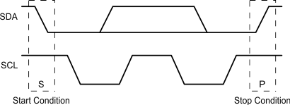
A controller sending a Start condition, a high-to-low transition on the SDA input/output, while the SCL input is high initiates I2C communication. After the Start condition, the device address byte is sent, most significant bit (MSB) first, including the data direction bit (R/W).
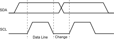
After receiving the valid address byte, this device responds with an acknowledge (ACK), a low on the SDA input/output during the high of the ACK-related clock pulse. On the I2C bus, only one data bit is transferred during each clock pulse. The data on the SDA line must remain stable during the high pulse of the clock period as changes in the data line at this time are interpreted as control commands (Start or Stop). The controller sends a Stop condition, a low-to-high transition on the SDA input/output while the SCL input is high.
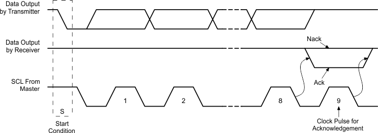
Any number of data bytes can be transferred from the transmitter to receiver between the Start and the Stop conditions. Each byte of eight bits is followed by one ACK bit. The transmitter must release the SDA line before the receiver can send an ACK bit. The device that acknowledges must pull down the SDA line during the ACK clock pulse, so that the SDA line is stable low during the high pulse of the ACK-related clock period. When a target receiver is addressed, it must generate an ACK after each byte is received. Similarly, the controller must generate an ACK after each byte that it receives from the target transmitter. Setup and hold times must be met to ensure proper operation.
A controller receiver signals an end of data to the target transmitter by not generating an acknowledge (NACK) after the last byte has been clocked out of the target. The controller receiver holding the SDA line high does this. In this event, the target transmitter must release the data line to enable the controller to generate a Stop condition.
Figure 8-36 shows the start and stop conditions of the transfer. Figure 8-37 shows the SDA and SCL signals for transferring a bit. Figure 8-38 shows a data transfer sequence with the ACK or NACK at the last clock pulse.
 Figure 8-36 I2C Definition of Start and Stop Conditions
 Figure 8-37 I2C Bit Transfer
 Figure 8-38 I2C Acknowledgment