JAJSVI4 October   2024 ADS127L21B

PRODUCTION DATA  

  1.   1
  2. 特長
  3. アプリケーション
  4. 概要
  5. Pin Configuration and Functions
  6. Specifications
    1. 5.1  Absolute Maximum Ratings
    2. 5.2  ESD Ratings
    3. 5.3  Recommended Operating Conditions
    4. 5.4  Thermal Information
    5. 5.5  Electrical Characteristics
    6. 5.6  Timing Requirements (1.65V ≤ IOVDD ≤ 2V)
    7. 5.7  Switching Characteristics (1.65V ≤ IOVDD ≤ 2V)
    8. 5.8  Timing Requirements (2V < IOVDD ≤ 5.5V)
    9. 5.9  Switching Characteristics (2V < IOVDD ≤ 5.5V)
    10. 5.10 Timing Diagrams
    11. 5.11 Typical Characteristics
  7. Parameter Measurement Information
    1. 6.1  Offset Error Measurement
    2. 6.2  Offset Drift Measurement
    3. 6.3  Gain Error Measurement
    4. 6.4  Gain Drift Measurement
    5. 6.5  NMRR Measurement
    6. 6.6  CMRR Measurement
    7. 6.7  PSRR Measurement
    8. 6.8  SNR Measurement
    9. 6.9  INL Error Measurement
    10. 6.10 THD Measurement
    11. 6.11 IMD Measurement
    12. 6.12 SFDR Measurement
    13. 6.13 Noise Performance
  8. Detailed Description
    1. 7.1 Overview
    2. 7.2 Functional Block Diagram
    3. 7.3 Feature Description
      1. 7.3.1 Analog Input (AINP, AINN)
        1. 7.3.1.1 Input Range
      2. 7.3.2 Reference Voltage (REFP, REFN)
        1. 7.3.2.1 Reference Voltage Range
      3. 7.3.3 Clock Operation
        1. 7.3.3.1 Internal Oscillator
        2. 7.3.3.2 External Clock
      4. 7.3.4 Modulator
      5. 7.3.5 Digital Filter
        1. 7.3.5.1 Wideband Filter
          1. 7.3.5.1.1 Wideband Filter Options
          2. 7.3.5.1.2 Sinc5 Filter Stage
          3. 7.3.5.1.3 FIR1 Filter Stage
          4. 7.3.5.1.4 FIR2 Filter Stage
          5. 7.3.5.1.5 FIR3 Filter Stage
          6. 7.3.5.1.6 FIR3 Default Coefficients
          7. 7.3.5.1.7 IIR Filter Stage
            1. 7.3.5.1.7.1 IIR Filter Stability
        2. 7.3.5.2 Low-Latency Filter (Sinc)
          1. 7.3.5.2.1 Sinc3 and Sinc4 Filters
          2. 7.3.5.2.2 Sinc3 + Sinc1 and Sinc4 + Sinc1 Cascade Filter
      6. 7.3.6 Power Supplies
        1. 7.3.6.1 AVDD1 and AVSS
        2. 7.3.6.2 AVDD2
        3. 7.3.6.3 IOVDD
        4. 7.3.6.4 Power-On Reset (POR)
        5. 7.3.6.5 CAPA and CAPD
      7. 7.3.7 VCM Output Voltage
    4. 7.4 Device Functional Modes
      1. 7.4.1 Speed Modes
      2. 7.4.2 Idle Mode
      3. 7.4.3 Standby Mode
      4. 7.4.4 Power-Down Mode
      5. 7.4.5 Reset
        1. 7.4.5.1 RESET Pin
        2. 7.4.5.2 Reset by SPI Register Write
        3. 7.4.5.3 Reset by SPI Input Pattern
      6. 7.4.6 Synchronization
        1. 7.4.6.1 Synchronized Control Mode
        2. 7.4.6.2 Start/Stop Control Mode
        3. 7.4.6.3 One-Shot Control Mode
      7. 7.4.7 Conversion-Start Delay Time
      8. 7.4.8 Calibration
        1. 7.4.8.1 OFFSET2, OFFSET1, OFFSET0 Calibration Registers (Addresses 0Ch, 0Dh, 0Eh)
        2. 7.4.8.2 GAIN2, GAIN1, GAIN0 Calibration Registers (Addresses 0Fh, 10h, 11h)
        3. 7.4.8.3 Calibration Procedure
    5. 7.5 Programming
      1. 7.5.1 Serial Interface (SPI)
        1. 7.5.1.1  Chip Select (CS)
        2. 7.5.1.2  Serial Clock (SCLK)
        3. 7.5.1.3  Serial Data Input (SDI)
        4. 7.5.1.4  Serial Data Output/Data Ready (SDO/DRDY)
        5. 7.5.1.5  SPI Frame
        6. 7.5.1.6  Full-Duplex Operation
        7. 7.5.1.7  Device Commands
          1. 7.5.1.7.1 No-Operation
          2. 7.5.1.7.2 Read Register Command
          3. 7.5.1.7.3 Write Register Command
        8. 7.5.1.8  Read Conversion Data
          1. 7.5.1.8.1 Conversion Data
          2. 7.5.1.8.2 Data Ready
            1. 7.5.1.8.2.1 DRDY
            2. 7.5.1.8.2.2 SDO/DRDY
            3. 7.5.1.8.2.3 DRDY Bit
            4. 7.5.1.8.2.4 Clock Counting
          3. 7.5.1.8.3 STATUS Byte
        9. 7.5.1.9  Daisy-Chain Operation
        10. 7.5.1.10 3-Wire SPI Mode
          1. 7.5.1.10.1 3-Wire SPI Mode Frame Reset
        11. 7.5.1.11 SPI CRC
      2. 7.5.2 Register Memory CRC
        1. 7.5.2.1 Main Program Memory CRC
        2. 7.5.2.2 FIR Filter Coefficient CRC
        3. 7.5.2.3 IIR Filter Coefficient CRC
  9. Register Map
  10. Application and Implementation
    1. 9.1 Application Information
      1. 9.1.1 SPI Operation
      2. 9.1.2 Input Driver
      3. 9.1.3 Antialias Filter
      4. 9.1.4 Reference Voltage
      5. 9.1.5 Simultaneous-Sampling Systems
    2. 9.2 Typical Applications
      1. 9.2.1 A-Weighting Filter Design
        1. 9.2.1.1 Design Requirements
        2. 9.2.1.2 Detailed Design Procedure
        3. 9.2.1.3 Application Curve
      2. 9.2.2 PGA855 Programmable Gain Amplifier
        1. 9.2.2.1 Design Requirements
        2. 9.2.2.2 Detailed Design Procedure
        3. 9.2.2.3 Application Curves
      3. 9.2.3 THS4551 Antialias Filter Design
        1. 9.2.3.1 Design Requirements
        2. 9.2.3.2 Detailed Design Procedure
        3. 9.2.3.3 Application Curves
    3. 9.3 Power Supply Recommendations
    4. 9.4 Layout
      1. 9.4.1 Layout Guidelines
      2. 9.4.2 Layout Example
  11. 10Device and Documentation Support
    1. 10.1 Documentation Support
      1. 10.1.1 Related Documentation
    2. 10.2 ドキュメントの更新通知を受け取る方法
    3. 10.3 サポート・リソース
    4. 10.4 Trademarks
    5. 10.5 静電気放電に関する注意事項
    6. 10.6 用語集
  12. 11Revision History
  13. 12Mechanical, Packaging, and Orderable Information

Reset by SPI Input Pattern

The device is also reset through SPI operation by inputting a long bit pattern. The input pattern is not part of the regular command format. CS must remain low for the entire bit sequence. There are two input patterns that can reset the ADC: pattern 1 and pattern 2. Pattern 1 consists of a minimum 1023 consecutive ones followed by one zero. The device resets on the falling edge of SCLK when the final zero is shifted in. This pattern is used for either 3- or 4-wire SPI modes. Figure 7-29 shows a pattern 1 reset example.
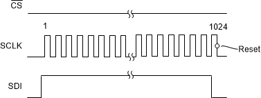
ADS127L21B Reset Pattern 1 (3-Wire or
                    4-Wire SPI Mode)Figure 7-29 Reset Pattern 1 (3-Wire or 4-Wire SPI Mode)

Reset pattern 2 is only used with the 4-wire SPI mode. To reset, input a minimum of 1024 consecutive ones (no ending zero value), followed by taking CS high, at which time reset occurs. Use pattern 2 when the devices are connected in daisy-chain mode. Figure 7-30 shows a pattern 2 reset example.
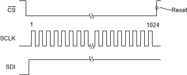
ADS127L21B Reset Pattern 2 (4-Wire SPI
                    Mode)Figure 7-30 Reset Pattern 2 (4-Wire SPI Mode)