JAJSVR9K December   2005  – December 2024 PCA9557

PRODUCTION DATA  

  1.   1
  2. 特長
  3. アプリケーション
  4. 概要
  5. Pin Configuration and Functions
  6. Specifications
    1. 5.1 Absolute Maximum Ratings
    2. 5.2 ESD Ratings
    3. 5.3 Recommended Operating Conditions
    4. 5.4 Thermal Information
    5. 5.5 Electrical Characteristics
    6. 5.6 I2C Interface Timing Requirements
    7. 5.7 Reset Timing Requirements
    8. 5.8 Switching Characteristics
    9. 5.9 Typical Characteristics
  7. Parameter Measurement Information
  8. Detailed Description
    1. 7.1 Functional Block Diagram
    2. 7.2 Feature Description
      1. 7.2.1 RESET
        1. 7.2.1.1 RESET Errata
          1. 7.2.1.1.1 System Impact
          2. 7.2.1.1.2 System Workaround
      2. 7.2.2 Power-On Reset
    3. 7.3 Programming
      1. 7.3.1 I2C Interface
    4. 7.4 Register Maps
      1. 7.4.1 Device Address
      2. 7.4.2 Control Register And Command Byte
      3. 7.4.3 Register Descriptions
        1. 7.4.3.1 Bus Transactions
          1. 7.4.3.1.1 Writes
          2. 7.4.3.1.2 Reads
  9. Application and Implementation
    1. 8.1 Application Information
    2. 8.2 Typical Application
      1. 8.2.1 Detailed Design Procedure
        1. 8.2.1.1 Minimizing ICC when I/O is Used to Control LED
    3. 8.3 Power Supply Recommendations
      1. 8.3.1 Power-On Reset Errata
        1. 8.3.1.1 System Impact
  10. Device and Documentation Support
    1. 9.1 Documentation Support
      1. 9.1.1 Related Documentation
    2. 9.2 Receiving Notification of Documentation Updates
    3. 9.3 サポート・リソース
    4. 9.4 Trademarks
    5. 9.5 静電気放電に関する注意事項
    6. 9.6 用語集
  11. 10Revision History
  12. 11Mechanical, Packaging, and Orderable Information

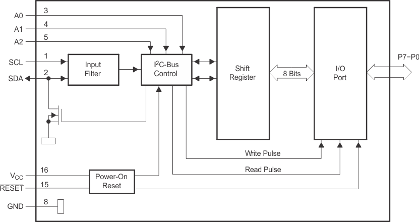
Functional Block Diagram

PCA9557 Logic
                    Diagram (Positive Logic)
Pin numbers shown are for the D, DB, DGV, PW, and RGY packages.
All I/Os are set to inputs at reset.
Figure 7-1 Logic Diagram (Positive Logic)
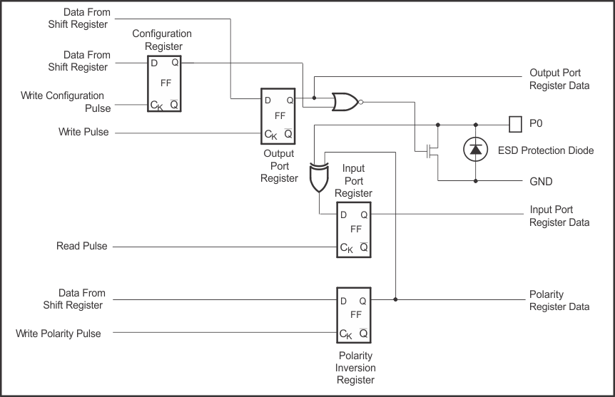
PCA9557 Simplified Schematic Diagram of P0
On power up or reset, all registers return to default values.
Figure 7-2 Simplified Schematic Diagram of P0
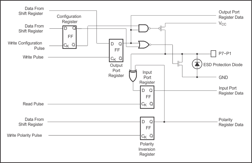
PCA9557 Simplified Schematic Diagram of P7–P1
On power up or reset, all registers return to default values.
Figure 7-3 Simplified Schematic Diagram of P7–P1