JAJU316G November 2016 – April 2020
3.3 DC Bus Regulation Loop
The DC bus regulation loop is assumed to be providing the power reference. This loop is divided by the square of the line voltages RMS to provide the conductance, which is further multiplied by the line voltage to give the instantaneous current command.
Small signal model of the DC bus regulation loop is developed by linearizing Equation 3 around the operating point.

For resistive load the bus voltage and current relate, as shown in Equation 4.

The DC voltage regulation loop control model can be drawn, as shown in Figure 6. An additional Vbus feedforward is applied to make the control loop independent of the bus voltage, and, thus, the plant model for the bus control can be written as shown in Equation 5.

Where:
- Hp_bus is the voltage loop plant as seen by the digital controller Gv.
- Output of the Gv is the power reference Po*
- vbus* is the voltage command/reference, vbus is the actual bus voltage.
- Co is the output capacitor, RL is the load resistance.
Using Figure 6, a proportional integrator (PI) compensator is designed for the voltage loop. The bandwidth of this loop is kept low as it is in conflict with the THD below steady state.

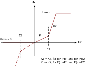
Additionally, a non-linear PI loop is used to reduce the transients in case of step load changes. Figure 7 shows the structure of the non-linear PI loop implemented on this design
