JAJU316G November 2016 – April 2020
6.4.4.3 Running Code (Build 4)
- Run the project by clicking.
- Raise the AC input to 120-Vrms VL-L and 208-Vrms VL-L, 60 Hz. A rectified current is going to be drawn from the input with PF close to 0.7 as shown in Figure 46.
- Bus voltage is set by the variable vBusRef and is set at 1.32 which corresponds to 600 V for this design.
- Start the PFC action by writing a 1 to clearTrip variable
- The board will now draw sinusoidal current and the PF will be close to 0.99 and THD will be around 2.5%. The scope capture will look as shown in Figure 47.
- The DC bus voltages will also be balanced, that is, guiVbusPM and guiVbusMN will be almost equal, which shows that the closed loop balance controller is working.
- SFRA is integrated in the software of this build to verify the designed compensator provides enough gain and phase margin by measuring on hardware. To run the SFRA keep the project running and from the syscfg page, click on the SFRA icon. SFRA GUI will pop-up.
- Select the options for the device on the SFRA GUI. For example for F28379D, select floating point. Click setup connection, and on the pop-up window ,uncheck the boot on connect option and select an appropriate COM port and Click OK. Return to the SFRA GUI and Click Connect.
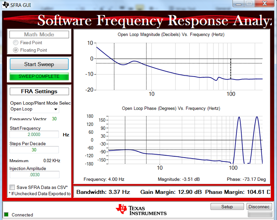
- The SFRA GUI will connect to the device. A SFRA sweep can now be started by clicking Start Sweep. The complete SFRA sweep will take a few minutes to finish. Activity can be monitored by seeing the progress bar on the SFRA GUI and also by checking the flashing of blue LED on the back on the control card that indicate UART activity. When complete a graph with the open loop plot will appear, as shown in Figure 48. This graph verifies that the designed compensator is indeed stable.
- The balance loop open loop gain is controlled by the variable Gs_GainKp and can be adjusted in case the BW is not enough. Though, for the balance loop, the bandwidth needs to be lower than the outer voltage loop and only 1 to 2 Hz of bandwidth is sufficient.
- Fully halting the MCU when in real-time mode is a two-step process. First, halt the processor by using the Halt button on the toolbar (
 ) or by using Target > Halt. Then take the MCU out of real-time mode by clicking on
  . Finally reset the MCU
 .
. - Close CCS debug session by clicking on Terminate Debug Session (Target > Terminate all).
 .
.
Figure 46. Build Level 4: Scope Capture IL1, IL2, IL3 and V1 (120Vrms L-N) with PWM Tripped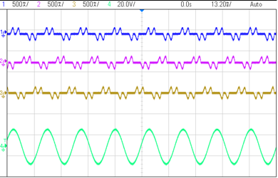

Figure 47. Build Level 4: Scope Capture IL1, IL2, IL3 and V1 (120-Vrms L-N) With Full PFC Build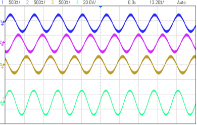

Figure 48. SFRA Run on Balance Voltage Loop