JAJU459B December 2017 – November 2022
- 概要
- リソース
- 特長
- アプリケーション
- 5
- 1System Description
-
2System Overview
- 2.1 Block Diagram
- 2.2
Design Considerations
- 2.2.1 Conditions of Use: Assumption
- 2.2.2
Diagnostics Coverage
- 2.2.2.1 Dual-Channel Monitoring
- 2.2.2.2 Checking ISO1211 Functionality With MCU (SIL1)
- 2.2.2.3 Checking TPS22919 Functionality With MCU (SIL1)
- 2.2.2.4 Checking TPS27S100 Functionality With MCU (SIL1)
- 2.2.2.5 Optional Monitoring Using RDY Pin of ISO5452, ISO5852S or UCC21750 Integrated Analog-to-PWM Isolated Sensor
- 2.2.3 Drive State
- 2.3 Highlighted Products
- 2.4 System Design Theory
-
3Hardware, Software, Testing Requirements, and Test Results
- 3.1 Getting Started Hardware
- 3.2 Testing and Results
- 4Design Files
- 5Related Documentation
- 6About the Author
- 7Recognition
- 8Revision History
2.4.1 Digital Input Receiver for STO
The ISO1211 receives 24-V digital signals and provides isolated digital outputs, without the requirement of a field-side power supply. External resists on the input signal path (R12 and R21) precisely set the limit for the current drawn from the field input. This current limit helps to minimize the power dissipated in the system. The current limit can be set for Type 1, 2, or 3 operation. The voltage transition thresholds are compliant with Type 1, 2, and 3 and can be increased further using an external resistor, R22 and R15. These two resistors are carbon MELF (pulse-proof) type used to prevent surge. For detailed test results, see the How to Design Isolated Digital Input Modules for Surge Immunity application brief.
Figure 2-10 shows a schematic of the ISO1211 receivers.
 Figure 2-10 ISO1211 Schematic
As per the specifications of the design, the voltage limits defined for an input voltage of 24 V is as follows:
- 15- to 30-V DC: STO function not engaged (motion allowed)
- 0- to 5-V DC: STO function engaged (motion inhibited)
These design requirements comply with Type 1 characteristics.
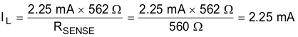
As Figure 2-10 shows, Type 1 operation uses a value of 560 Ω for R12 and R21 and results in a current limit of 2.25 mA (typical). The relationship between the RSENSE resistor and the typical current limit (IL) is given by Equation 1.
Resistors R22 and R15 set the voltage thresholds (VIH and VIL) in addition to limiting the surge current. Use a resistor of 2.5 kΩ for R22 and R15 for a Type 1 system. Equation 2 and Equation 3 are used to calculate the typical VIH and VIL values, respectively.
Note that the specific assumption of input signals STO_1 and STO_2 is that the input voltage is between 0-V and 24-V nominal with worst case of 3.6-V as logic low and 20.4-V as logic high. Logic high range is 24-V DC ±15% (nominal) with ±60-V DC absolute maximum. No intermediate voltage is expected.
As per the design specifications, low STO pulses that are less than 1 ms are rejected. Address this rejection by placing a low-pass filter at the output signals of the ISO1211 device. To meet the design requirements, place an RC combination with R = 1 k and C = 3.3 μF (see Equation 4).

The cutoff frequency of this filter is 48 Hz, where:
- V(t) = 3.3
- At t = 1 ms
- V(t) = 2.8 V, which is within the logic threshold high range of the AND gate.
For implementation, use 2 × 499 Ω R17 and R20 in series for STO 1 and use 2 × 499 Ω R6 and R13 in series for STO 2. This is to get rid of the short or change value failure mode of resistor which will bypass the filter for logic gate input.