JAJU510H March   2018  – December 2022


  1.   概要
  2.   リソース
  3.   特長
  4.   アプリケーション
  5.   5
  6. 1System Description
    1. 1.1 Key System Specifications
  7. 2System Overview
    1. 2.1 Block Diagram
    2. 2.2 Highlighted Products
      1. 2.2.1  UCC21710
      2. 2.2.2  UCC5320
      3. 2.2.3  TMS320F28379D
      4. 2.2.4  AMC1305M05
      5. 2.2.5  OPA4340
      6. 2.2.6  LM76003
      7. 2.2.7  PTH08080W
      8. 2.2.8  TLV1117
      9. 2.2.9  OPA350
      10. 2.2.10 UCC14240
    3. 2.3 System Design Theory
      1. 2.3.1 Three-Phase T-Type Inverter
        1. 2.3.1.1 Architecture Overview
        2. 2.3.1.2 LCL Filter Design
        3. 2.3.1.3 Inductor Design
        4. 2.3.1.4 SiC MOSFETs Selection
        5. 2.3.1.5 Loss Estimations
        6. 2.3.1.6 Thermal Considerations
      2. 2.3.2 Voltage Sensing
      3. 2.3.3 Current Sensing
      4. 2.3.4 System Power Supplies
        1. 2.3.4.1 Main Input Power Conditioning
        2. 2.3.4.2 Isolated Bias Supplies
      5. 2.3.5 Gate Drivers
        1. 2.3.5.1 1200-V SiC MOSFETs
        2. 2.3.5.2 650-V SiC MOSFETs
        3. 2.3.5.3 Gate Driver Bias Supply
      6. 2.3.6 Control Design
        1. 2.3.6.1 Current Loop Design
        2. 2.3.6.2 PFC DC Bus Voltage Regulation Loop Design
  8. 3Hardware, Software, Testing Requirements, and Test Results
    1. 3.1 Required Hardware and Software
      1. 3.1.1 Hardware
        1. 3.1.1.1 Test Hardware Required
        2. 3.1.1.2 Microcontroller Resources Used on the Design
        3. 3.1.1.3 F28377D, F28379D Control-Card Settings
      2. 3.1.2 Software
        1. 3.1.2.1 Getting Started With Firmware
          1. 3.1.2.1.1 Opening the CCS project
          2. 3.1.2.1.2 Digital Power SDK Software Architecture
          3. 3.1.2.1.3 Interrupts and Lab Structure
          4. 3.1.2.1.4 Building, Loading and Debugging the Firmware
        2. 3.1.2.2 Protection Scheme
        3. 3.1.2.3 PWM Switching Scheme
        4. 3.1.2.4 ADC Loading
    2. 3.2 Testing and Results
      1. 3.2.1 Lab 1
      2. 3.2.2 Testing Inverter Operation
        1. 3.2.2.1 Lab 2
        2. 3.2.2.2 Lab 3
        3. 3.2.2.3 Lab 4
      3. 3.2.3 Testing PFC Operation
        1. 3.2.3.1 Lab 5
        2. 3.2.3.2 Lab 6
        3. 3.2.3.3 Lab 7
      4. 3.2.4 Test Setup for Efficiency
      5. 3.2.5 Test Results
        1. 3.2.5.1 PFC Mode - 230 VRMS, 400 V L-L
          1. 3.2.5.1.1 PFC Start-up – 230 VRMS, 400 L-L AC Voltage
          2. 3.2.5.1.2 Steady State Results at 230 VRMS, 400 V L-L - PFC Mode
          3. 3.2.5.1.3 Efficiency and THD Results at 220 VRMS, 50 Hz – PFC Mode
          4. 3.2.5.1.4 Transient Test With Step Load Change
        2. 3.2.5.2 PFC Mode - 120 VRMS, 208 V L-L
          1. 3.2.5.2.1 Steady State Results at 120 VRMS, 208 V-L-L - PFC Mode
          2. 3.2.5.2.2 Efficiency and THD Results at 120 VRMS - PFC Mode
        3. 3.2.5.3 Inverter Mode
          1. 3.2.5.3.1 Inverter Closed Loop Results
          2. 3.2.5.3.2 Efficiency and THD Results - Inverter Mode
          3. 3.2.5.3.3 Inverter - Transient Test
      6. 3.2.6 Open Loop Inverter Test Results
  9. 4Design Files
    1. 4.1 Schematics
    2. 4.2 Bill of Materials
    3. 4.3 PCB Layout Recommendations
      1. 4.3.1 Layout Prints
    4. 4.4 Altium Project
    5. 4.5 Gerber Files
    6. 4.6 Assembly Drawings
  10. 5Trademarks
  11. 6About the Authors
  12. 7Revision History

Lab 4

In this lab the power stage is run in a closed loop with grid connection on HIL platform. Figure 3-14 shows the SW diagram.

Figure 3-14 Lab 4 Software Diagram
Note: This lab is only verified under HIL setup

Set the project to Lab 4 by changing the Lab Number in the <settings.h> file, (this will be changed by powerSUITE GUI when using powerSUITE project).

In the user settings.h file some additional options are available, but the following are used for the tests documented in this user guide.

#if TINV_LAB == 4
#define TINV_TEST_SETUP TINV_TEST_SETUP_GRID_CONNECTED
#define TINV_PROTECTION TINV_PROTECTION_ENABLED
#define TINV_SFRA_TYPE TINV_SFRA_CURRENT
#define TINV_SFRA_AMPLITUDE (float32_t)TINV_SFRA_INJECTION_AMPLITUDE_LEVEL2
#define TINV_POWERFLOW_MODE TINV_INVERTER_MODE
#define TINV_DC_CHECK 0
#define TINV_SPLL_TYPE TINV_SPLL_SRF
#endif

Lab 4

In this check, the SW is run on the HIL platform.

Build and load the code, use the lab4.js file to populate the watch variables in the CCS window.

  • Slowly ramp the DC bus voltage 'Vbus' to 800 V
  • Enter "1" on TINV_startPowerStage variable and ramp the AC voltage of the grid to 230Vrms, L-N; that is, 400 VL-L
  • Set up an appropriate grid connection and turn on the relay by writing a 1 to TINV_allRelaySet as soon as voltage reaches 230 VRMS as the inrush current limit resistors might get heated and burn out. The current should now be fed into the grid.
  • Slowly increase this TINV_idRef_pu variable to be 0.6 pu, at this point the per phase power will be approximately 1.9 kW

Measure the current loop bandwidth using SFRA. Figure 3-15 and Figure 3-16 show plant response and loop response of inverter operating in current mode measured on the HIL platform.
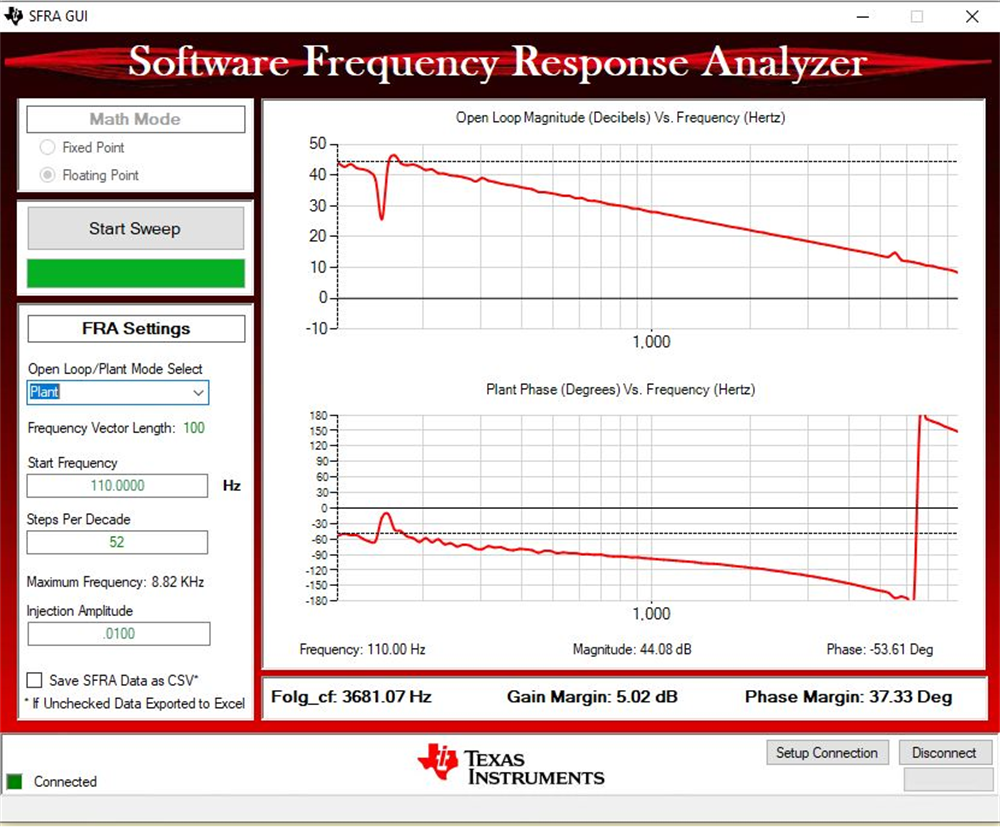
GUID-20210408-CA0I-3ZTL-2KS5-MXZCKWP1JT5L-low.pngFigure 3-15 Inverter SFRA Plant Response Measured on HIL
GUID-20210408-CA0I-SPRP-1JLB-SJXTSC7TTSZH-low.pngFigure 3-16 Inverter SFRA Loop Response Measured on HIL