JAJU510H March 2018 – December 2022
- 概要
- リソース
- 特長
- アプリケーション
- 5
- 1System Description
- 2System Overview
-
3Hardware, Software, Testing Requirements, and Test Results
- 3.1 Required Hardware and Software
- 3.2 Testing and Results
- 4Design Files
- 5Trademarks
- 6About the Authors
- 7Revision History
3.2.3.1 Lab 5
This is the first PFC lab. In this lab sensing is checked and no switching action occurs until clearPWMTrip is set to 1.
The hardware setup for the PFC mode is explained in Figure 3-17. TI recommends starting the PFC at low voltage like 30 VRMS and connecting a 2-kΩ resistor.
Set the project to Lab 5 by changing the Lab Number in the <settings.h> file, (this will be changed by powerSUITE GUI when using powerSUITE project).
Under this condition, the converter operates as a rectifier and rectified current can be observed being drawn without any power factor correction. SPLL locking can also be safely verified in this build.
Hence, the following variables are put on the datalogger:
TINV_dVal1 = TINV_vGrid_A_sensed_pu;
TINV_dVal2 = TINV_angleSPLL_radians / (float32_t)(2.0f * TINV_PI);
TINV_dVal3 = TINV_vGrid_A_sensed_pu;
TINV_dVal4 = TINV_iInv_A_sensed_pu;
DLOG_4CH_run(&TINV_dLog1);
Make sure the Grid frequency is specified correctly, the grid frequency can be changed through the sysconfig page for powerSUITE based projects. If not powerSUITE based project one can modify the tinv_settings.h file.
#define TINV_AC_FREQ_HZ ((float32_t)50)Build and load the code, use the lab5.js file to populate the watch variables in the CCS window.
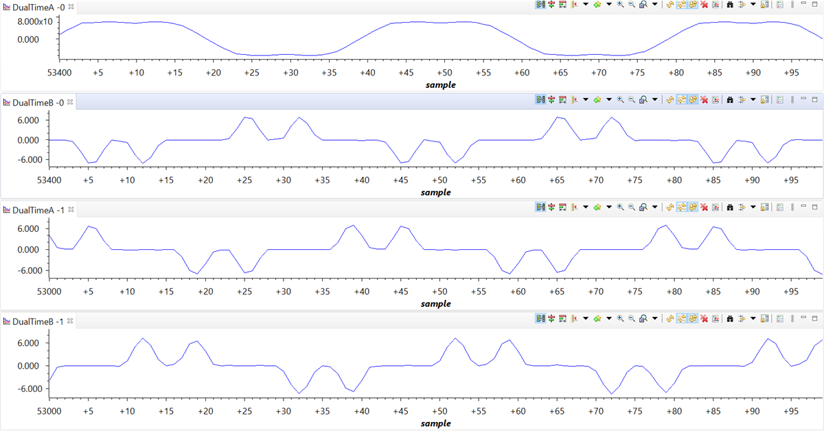
PLL lock can be checked by plotting the buffers, use the graph1.graphprop to see the buffer through Tools→ Graph → Dual Time.
Cosine transforms are used hence the angle will be 0 when the Vgrid as its peak.
First close the relay by writing a 1 to TINV_allRelaySet
Initially, the test may be run with only 30 VRMS for safety, hence safely ramp the AC supply to 30 VRMS and observe the graph in the CCS debug window to confirm the PLL is locking. Figure 3-19 shows low voltage phase locked loop check from watch window.
 Figure 3-19 PLL - Grid Voltage
Synchronization
Figure 3-19 PLL - Grid Voltage
SynchronizationIf the PLL is not locking one may also issue a tinv_reset_PLL command by setting it to 1, this will initiate a task to zero out an integrated error in the module and zero all the memory elements.
Similarly, the current flowing from the grid across all phases can be checked, using the graph watch window of CCS. Figure 3-20 shows the Sensed grid currents from graph windowCheck for three phase grid currents observed from the watch window.
 Figure 3-20 Sensed Grid Currents - PFC
Mode
Figure 3-20 Sensed Grid Currents - PFC
ModeTo verify boost action in Lab 5, follow the steps according to the sequence provided:
- Turn on the auxiliary power supply and set it to 15 V and then debug and run the code.
- Connect suitable load to the terminals J1 and J2. Make sure to use a high load resistance (around 2 kΩ) which otherwise can lead to high inrush currents triggering the overcurrent flag.
- Apply 30 VRMS AC voltage to the three phase terminals
- Immediately turn on the relay by writing a 1 to TINV_allRelaySet. Voltage should now start to appear across the DC terminals.
- Clear the PWM trip by setting TINV_clearPwmTrip to 1 to see a slight boost in DC voltage.
Before PFC action begins, a rectified current will be drawn due to the load on the Vbus. As soon as clearPWMTrip is set to 1, a slight boost in DC voltage is seen. Note the input current has a double bump without the neutral connected to the source at light load.
There can be a situation in the labs for PFC (Lab 5, Lab 6, and Lab 7) where the converter operates as a rectifier and rectified current is seen being drawn without any power factor correction. But as soon as TINV_clearPwmTrip is set to 1, there is no switching action – the Gate Signals remain off.
This is because there is an overcurrent or DSAT flag (InvA_overcurrent, InvB_overcurrent,DSATA, DSATB) which is set in one of the three phases and this happens under three circumstances:
- On closing the relays, there is an inrush current which creates an overcurrent trip in one of the three phases.
- When TINV_clearPwmTrip to 1, the switching action causes one of the flags to be set.
- Setting TINV_StartpowerStage to 1 for closing the current and voltage loop.
The EPWM TZFLG is set to 0X000C and under this condition no switching occurs. So make sure the load resistance is increased so that the inrush currents will not cause a trip condition and the EPWM TZFLG changes from 0x0004 to 0x0000 and switching occurs.
Once the FLG is set to 0x000C, even if we do a TINV_reset_fault_status to reset the faults, though the faults may be cleared PWM action will not be observed.
The goal is, as soon as the auxiliary power supply is started and the code debugged, all the faults – namely InvA_overcurrent, InvB_overcurrent, DSATA, DSATB; and so forth – should be set to zero so that the controller does not go into a trip state.