JAJU510H March 2018 – December 2022
- 概要
- リソース
- 特長
- アプリケーション
- 5
- 1System Description
- 2System Overview
-
3Hardware, Software, Testing Requirements, and Test Results
- 3.1 Required Hardware and Software
- 3.2 Testing and Results
- 4Design Files
- 5Trademarks
- 6About the Authors
- 7Revision History
3.2.3.3 Lab 7
In this build level the voltage and current loop for the PFC is checked. Here the variable TINV_vBusRef_pu is defined to set the voltage at which the output DC bus voltage is to be regulated.
Figure 3-30 describes the software flow for running Lab 7.
Set the project to Lab 7 by changing the Lab Number in the <settings.h> file, (this will be changed by powerSUITE GUI when using powerSUITE project).
In the user settings.h file some additional options are available, but the following code is used for the tests documented in this user guide.
#if TINV_LAB == 7
#define TINV_TEST_SETUP TINV_TEST_SETUP_RES_LOAD
#define TINV_PROTECTION TINV_PROTECTION_ENABLED
#define TINV_SFRA_TYPE TINV_SFRA_CURRENT
#define TINV_SFRA_AMPLITUDE (float32_t)TINV_SFRA_INJECTION_AMPLITUDE_LEVEL2
#define TINV_POWERFLOW_MODE TINV_RECTIFIERER_MODE
#define TINV_DC_CHECK 0
#define TINV_SPLL_TYPE TINV_SPLL_SRF
#endif
In this check the SW is run on the hardware, or the HIL platform, or both.
Refer to the hardware test set up section for actual details of the equipment used for configuring the test. At this time, do not supply any HV power to the board.
- First launch the main.cfg and select Lab 7 in the project options. The compensator style (PI compensator) and the tuning loop (current loop) will be automatically populated. Now click run compensation designer icon and compensation designer tool will launch, with the model of the current loop plant with parameters specified on the powerSUITE page.
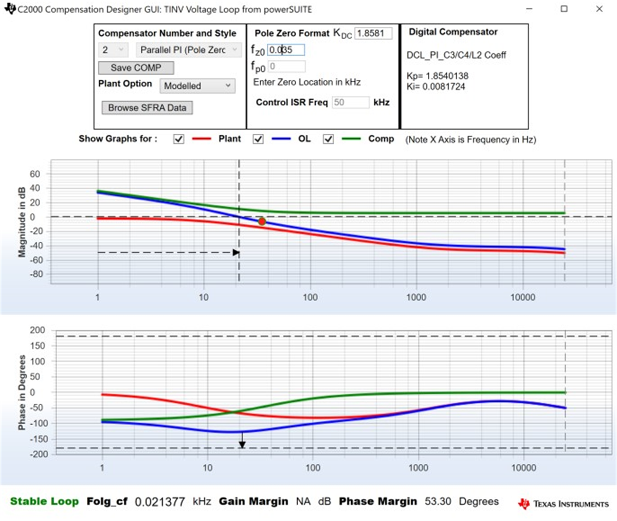
- Figure 3-31 shows the current compensator coefficients used for running the control loop. The user can modify these coefficients to meet the necessary loop bandwidth and phase margin. The ideal coefficients with resistive load are slightly different than the one used for grid connection because the grid impedance is very low. The compensator design transfer function and response will be as shown in Figure 3-31.
#define TINV_GI_PI_KP ((float32_t)1.8540138247))
#define TINV_GI_PI_KI ((float32_t)0.0081723506))
Figure 3-31 Compensator Design GUI - Voltage Loop PI Coefficients
 - Once satisfied with the proportional and integral gain values, click on Save COMP. This will save the compensator values into the project. Close the Compensation Designer, and return to the powerSUITE page.
- Turn on the auxiliary power supply and set it to 15 V. Build and load the code, use the lab7.js file to populate the watch variables in the CCS window.
- Set the load resistance to a high value 3.18 kΩ.
- Set the AC input voltage to 230 VRMS with appropriate current limit.
- After turning on the ac power supply, immediately turn on the relay by writing a 1 to TINV_allRelaySet. Ensure that the relay is turned on immediately (within 3-4 seconds) after turning on the AC supply.
- Now set TINV_vBusRef_pu to 0.684 pu. This corresponds to bus voltage of 800 V
- To start the PFC mode, enter "1" on TINV_startPowerStage variable, the current should now be drawn from the grid as a sinusoidal signal (with some harmonics as it is at low power) and boost action seen on the vBus. The output voltage will boost from 550 V to around 800 V drawing around 250 W power from AC supply as shown in Figure 3-32. This transition happens in around 150 ms.
- The current will become sinusoidal as the load is increased. This verifies start up of PFC at 230 VRMS and is shown in Figure 3-32.
- In case any overcurrent trip is observed which causes the PWMs to switch off, please refer the notes in Lab 5 to debug this condition.
- The converter efficiency results and transient tests are shown in the Test Results section.
- SFRA is integrated in the software of this lab to verify the designed compensator provides enough gain and phase margin by measuring on hardware. To run the SFRA keep the project running, and from the cfg page, click on the SFRA icon. SFRA GUI will pop up.
- Select the options for the device on the SFRA GUI. For example, for F28377D select floating point. Click on Setup Connection. On the pop-up window uncheck the boot on connect option, and select an appropriate COM port. Click OK. Return to the SFRA GUI, and click Connect.
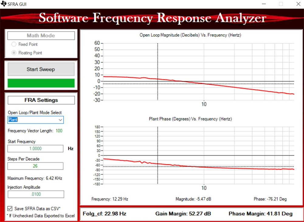
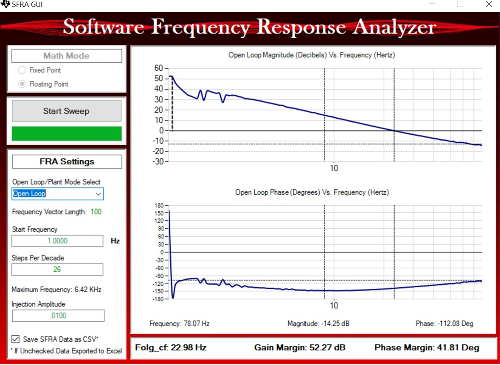
- The SFRA GUI will connect to the device. A SFRA sweep can now be started by clicking Start Sweep. The complete SFRA sweep will take a few minutes to finish. Activity can be monitored by seeing the progress bar on the SFRA GUI and also checking the flashing of blue LED on the back on the control card that indicates UART activity. Once complete, a graph with the open loop plot will appear, as in Figure 3-32. Figure 3-32 shows measured plant response by SFRA GUI and Figure 3-33 shows measured loop response by SFRA GUI. This verifies that the designed compensator is indeed stable.
 Figure 3-32 PFC SFRA Plant Response for Voltage Loop
 Figure 3-33 PFC SFRA Loop Response for Voltage Loop
- The frequency response data is also saved in the project folder under an SFRA data folder and is time stamped with the time of the SFRA run. Also, note the measured gain and phase margin are close to the modelled values as shown in the voltage loop compensator design as previously elaborated.
- This action verifies the voltage loop compensator design. To bring the system to a safe stop, bring the input AC voltage down to zero.