JAJU510H March 2018 – December 2022
- 概要
- リソース
- 特長
- アプリケーション
- 5
- 1System Description
- 2System Overview
-
3Hardware, Software, Testing Requirements, and Test Results
- 3.1 Required Hardware and Software
- 3.2 Testing and Results
- 4Design Files
- 5Trademarks
- 6About the Authors
- 7Revision History
2.3.1.1 Architecture Overview
To understand the impetus behind a three level t-type inverter, some background on a traditional two-level inverter is required. A typical implementation of this architecture is shown in Figure 2-11.
 Figure 2-11 Two-Level, Three-Phase Inverter Architecture
To simplify the analysis, a single leg can be isolated.
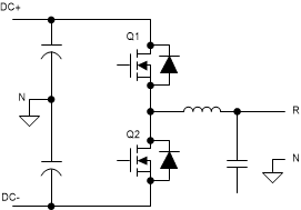 Figure 2-12 Two-Level, Single-Phase Inverter Leg
In this example, the two switching devices as a pair have four possible conduction states, independent of the other phases:
 Figure 2-13 Q1 and Q2 off
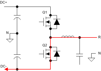 Figure 2-15 Q1 off, and Q2 on
 Figure 2-14 Q1 on, and Q2 off
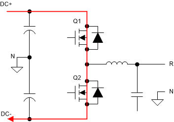 Figure 2-16 Q1 and Q2 on (Invalid)
By observing the current path through the inverter, each switching device must be capable of blocking the full DC link voltage present between DC+ and DC–. In traditional low-voltage systems (< 600 V), this capability is fairly trivial with common off-the-shelf IGBTs. However, if the DC link voltage is pushed higher to increase the power throughput without increasing current, as is a common trend in power electronics, this limitation puts an upper level on the supported voltage ranges.
Additionally, the increased voltage does result in increased switching losses in the traditional IGBTs. The low dV/dt exacerbates itself in these devices, even if they are able to support the higher voltages. This dV/dt is what determines how quickly one device can transition from on to off (or vice versa), thus dictating the dead time between each of these states. An elongated switch time or dead time means the switches spend less time at full conduction, resulting in decreased efficiency.
These two primary drawbacks of a two-level inverter are what drives the implementation in this design.
The next step up from a standard two-level inverter is a T-type three-level inverter. This type is implemented by inserting two back-to-back switching devices between the switch node and the neutral point of the DC link created by the bulk input capacitors. These two switch devices are placed in a common emitter configuration so that current flow can be controlled by switching one or the other on or off. This configuration also enables both of them to share a common bias supply as the gate-emitter voltage is identically referenced. Figure 2-17 shows a simplified view of the implementation.
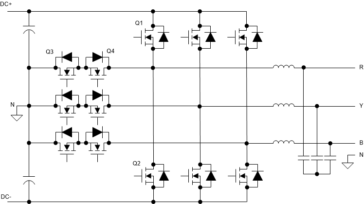 Figure 2-17 Three-Level T-Type, Three-Phase Inverter Architecture
To assist in understanding the benefits of the architecture, the inverter is again reduced to a single leg.
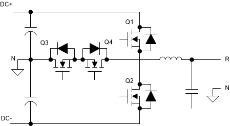 Figure 2-18 Three-Level T-Type, Single-Phase Inverter Leg
Adding two extra switching devices complicates the control of the system, but the same process of evaluating current flow during various modulation points illustrates the architecture benefits. Additionally, a simplified commutation scheme can be demonstrated, illustrating that control of a T-type inverter is not substantially more difficult than a traditional two-level architecture.
A single leg has three potential connection states: DC+, DC–, or N. This connection can be accomplished by closing Q1, closing Q3 and Q4, and closing Q2, respectively. However, this scheme depends on the current path in the system. Rather, for a DC+ connection, Q1 and Q3 can be closed, Q2 and Q4 for a neutral connection, and Q2 and Q4 for a DC– connection. This scheme acts independent of current direction as shown in the following figures.
 Figure 2-19 Q1 on, Q2 off, Q3 on, and Q4 off
 Figure 2-21 Q1 off, Q2 off, Q3 on, and Q4 on
 Figure 2-20 Q1 off, Q2 off, Q3 on, and Q4 off
This example starts with the output phase connected to DC+ by closing Q1 and Q3, resulting in current output from the system. To transition to an N connection, Q1 is opened and after a dead-time delay, and Q4 is closed. This setup allows current to naturally flow through Q3 and the diode of Q4.
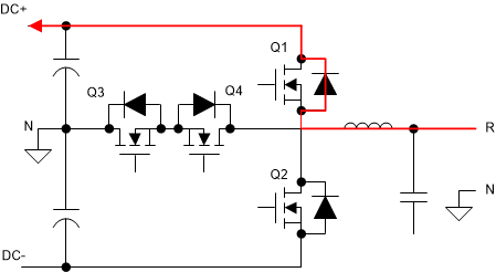 Figure 2-22 Q1 on, Q2 off, Q3 on, and Q4 off
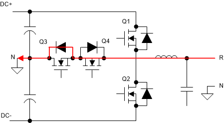 Figure 2-24 Q1 off, Q2 off, Q3 on, and Q4 on
 Figure 2-23 Q1 off, Q2 off, Q3 on, and Q4 off
For a negative current, the same sequence can be used. Once Q4 is closed, current then flows through it and the diode of Q3 rather than the diode of Q1.
 Figure 2-25 Q1 off, Q2 off, Q3 on, Q4 on
 Figure 2-27 Q1 on, Q2 off, Q3 on, Q4 off
 Figure 2-26 Q1 off, Q2 off, Q3 on, Q4 off
A similar natural current flow can be observed when connecting the output leg from N to DC+ with a positive current. Q3 and Q4 start closed with a full N connection. Q4 is switched off, but current still flows through its associated diode. Closing Q1 now naturally switches the current flow from N to DC+.
 Figure 2-28 Q1 off, Q2 off, Q3 on, Q4 on
 Figure 2-30 Q1 on, Q2 off, Q3 on, Q4 off
 Figure 2-29 Q1 off, Q2 off, Q3 on, Q4 off
As in the earlier example when moving from a DC+ to N connection on a negative current, the same scheme can also be used here for a positive current. Q3 and Q4 begin closed, conducting current into N. Q4 is opened, causing current to flow through the diode of Q1. Lastly, Q1 is closed, and current remains flowing in the same direction.
All four of these transition states (DC+ to N, N to DC+, with both forward and reverse current) all share two simple switching schemes. This also holds true for transitions to and from DC– through Q2. By maintaining this scheme through all switching cycles, a simple dead-zone delay between switching events is all that is needed to avoid shoot-though; however, additional protection can be added in the control software with relative ease.
An additional benefit from this modulation scheme is that Q3 and Q4 never switch at the same time. This benefit reduces voltage stress on the devices as well as the power rating of the bias supply to drive these devices effectively. As mentioned earlier, Q3 and Q4 can share a single supply sized for one driver rather than two.
Q1 and Q2 still need to block the full DC link voltage as they would in the traditional architecture. To use a higher DC bus voltage, full-voltage FETs still need to be in place here; however, because they are back to back and do not switch at the same time, the two switches on the center leg can be at a lower rating.