JAJU528B August 2022 – January 2023 OPA388-Q1
- 概要
- リソース
- 特長
- アプリケーション
- 5
- 1System Description
- 2System Overview
- 3Hardware, Testing Requirements, and Test Results
- 4Design Files
- 5Software Files
- 6Related Documentation
- 7Trademarks
- 8Revision History
2.2.3 SN6501-Q1
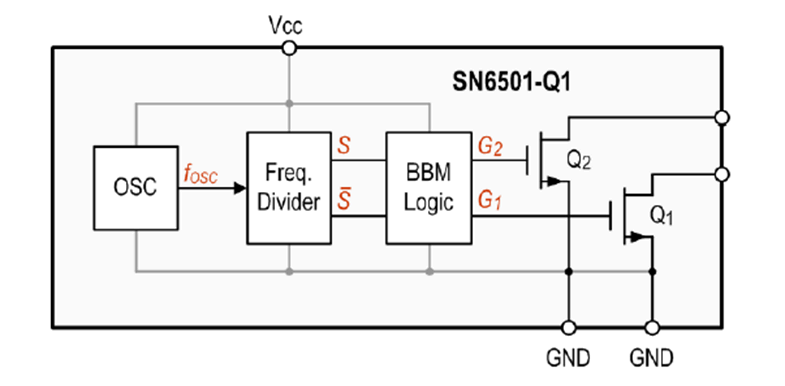
The SN6501-Q1 is a transformer driver designed for low-cost, small form-factor, isolated DC/DC converters using push-pull topology. The device includes an oscillator that feeds a gate drive circuit. The gate drive, comprising a frequency divider and a break-before-make (BBM) logic, provides two complementary output signals that alternately turn the two output transistors ON and OFF. The output frequency of the oscillator is divided down by an asynchronous divider that provides two complementary output signals with a 50% duty cycle. A subsequent BBM logic inserts a dead time between the high-pulses of the two signals. The resulting output signals present the gate-drive signals for the output transistors. As shown in Figure 2-5, before either one of the gates can assume logic high, there must be a short time period during which both signals are low and both transistors are high impedance. Known as BBM time, this short period is required to avoid shorting out both ends of the primary.
 Figure 2-5 SN6501-Q1 Block
Diagram
Figure 2-5 SN6501-Q1 Block
DiagramKey features include:
- AEC-Q100 qualified with –40°C to +125°C ambient operating temperature
- Push-pull driver for small transformers
- High primary-side current drive, 5-V supply: 350 mA (max)
- High primary-side current drive, 3.3-V supply: 150 mA (max)
- Low ripple on rectified output permits small output capacitors
- Small 5-pin SOT-23 package