JAJU633 October 2018
- 概要
- リソース
- 特長
- アプリケーション
- デザイン・イメージ
- 1System Description
-
2System Overview
- 2.1 Block Diagram
- 2.2 Highlighted Products
- 2.3 LM74700
- 2.4
System Design Theory
- 2.4.1
Design Procedure
- 2.4.1.1 Operating Parameters, Duty Cycle
- 2.4.1.2 Setting the Switching Frequency
- 2.4.1.3 Inductor Value Calculation
- 2.4.1.4 Peak Inductor Current
- 2.4.1.5 Calculating RIS (R9)
- 2.4.1.6 Minimum Output Capacitance
- 2.4.1.7 Setting the LED Current
- 2.4.1.8 Soft-Start Capacitor
- 2.4.1.9 Overvoltage Protection (OVP)
- 2.4.1.10 Main N-Channel MOSFET Selection
- 2.4.1.11 Rectifier Diode Selection
- 2.4.1.12 Thermal Protection
- 2.4.2 Designing for Low EMI
- 2.4.1
Design Procedure
- 3Hardware, Software, Testing Requirements, and Test Results
- 4Design Files
- 5Related Documentation
2.4.2.1 EMI Performance
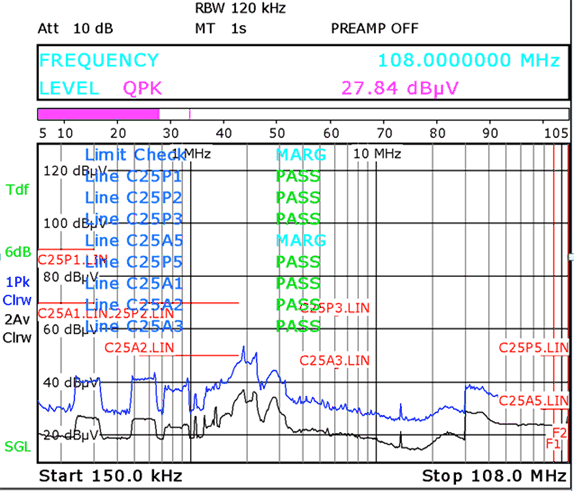
Figure 5 shows the passing conducted EMI scan for this design at a nominal 13 V input voltage and driving a 14 LEDs load in both high-beam and low-beam mode (seven LEDs in series for low beam and seven LEDs in series for high beam) at 1.25 A of LED current. The blue trace is the peak scan, and the line labeled C25Px denotes the peak limits for CISPR-25 Class 3. The black trace is the average scan with the line labeled "C25Ax" denoting average limits for CISPR-25 Class 3. The scan covers the entire conducted frequency range from 150 kHz to 108 MHz.
This performance by board layout only and without shielding. This pre-compliance test scan is used for engineering development and evaluation and not a certified EMI test result. If an official EMI test result is required, it is the responsibility of the end-user to submit any design based on this reference design to a certified EMI lab.
 Figure 5. CISPR-25 Class 3 Conducted EMI Scan (C25Px: Peak Limits, C25Ax: Average Limits)
No Shielding: VIN = 13 V, VF = 44 V, ILED = 1.25 A (Pre-Compliance Data)
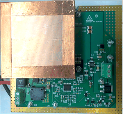
 Figure 6. Shielding is required on Switching Components to pass CISPR-25 Class 5 Conducted EMI
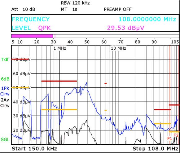
  Figure 7. CISPR-25 Class 5 Conducted EMI Scan (C25Px: Peak Limits, C25Ax: Average Limits)
VIN = 13 V, VF = 44 V, ILED = 1.25 A (Pre-Compliance Data)