JAJU785A January 2017 – March 2020
3.2.3.2.2.6 Run the Code
- Run the code by using the <F8> key or the Run button on the toolbar.
- Please use a load of at least 2 A or higher (within board specifications) at the 12-V output. If this is the first time of running closed loop test on this board, select a load between 5 A and 15 A.
- Set the 400-V DC supply to output 390 V. Set the power supply current limit to an appropriate level for this test. Now turn ON this 390-V power supply.
- At this point the output voltage should still be zero as the converter start command has not been initiated.
- Now set theLLC_startFlag to 1 in the Expressions Window.
- The converter operation should start and the output should ramp-up to approximately 12 V.
- Observe the effect of varying load on the output voltage and input current. There should be virtually no effect on the output voltage. Similarly observe the effect of varying the input voltage. Again there should be virtually no effect on the output voltage. (1)
- Different waveforms, like the PWM gate drive signals, input voltage, and current and output voltage may also be probed using an oscilloscope. Appropriate safety precautions should be taken and appropriate grounding requirements should be considered while probing these high voltages and high currents for this isolated DC-DC converter.
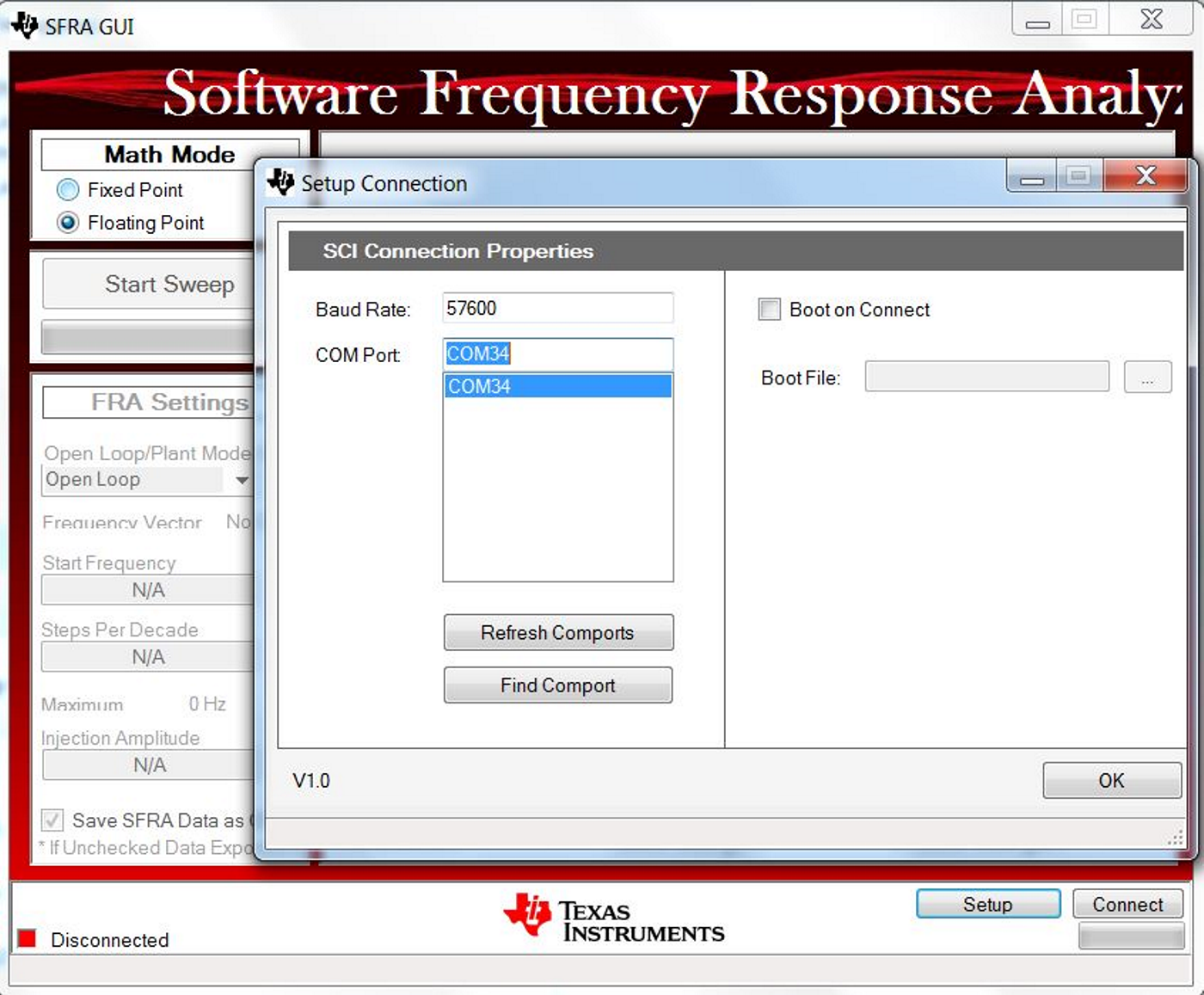
- Now click on main.syscfg file and open SFRA. Click on setup connection, and select the appropriate COM port. Make sure that the baud rate is set to 57600 and that Boot on Connect is unchecked. Click OK.
- Select Floating Point math.
- Click Connect on the SFRA GUI. Once the GUI is connected, click on Start Sweep. SFRA will start applying different frequencies and collecting the response for frequency analysis. The effect of this process may be seen on the output voltage as observed on an oscilloscope. The high-frequency signals riding on the output voltage indicate an active SFRA run.
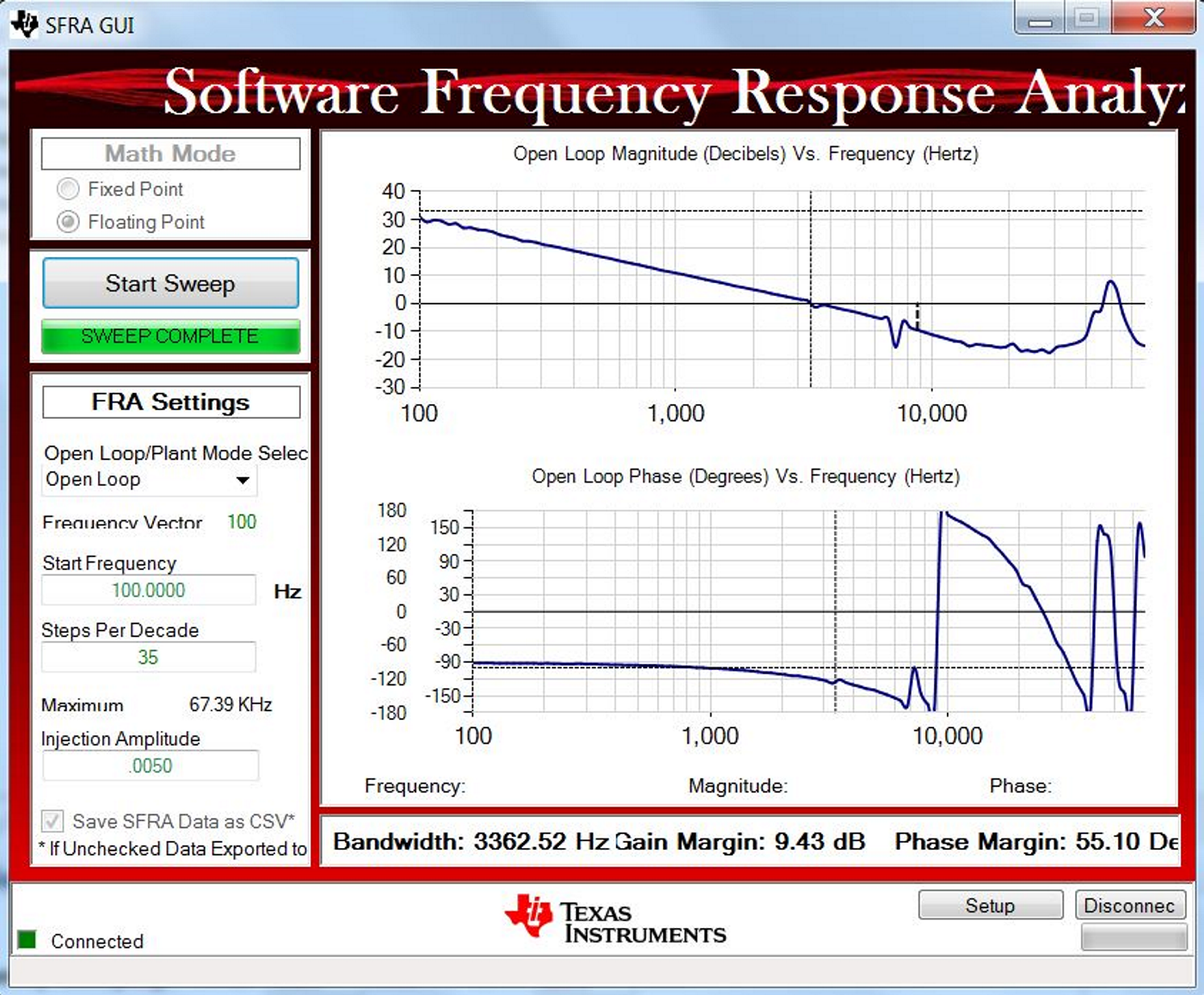
- Once the frequency sweep is complete, the response will be displayed on the SFRA GUI. The bandwidth, gain margin, and phase margin should be similar to the values noted on the Compensation Designer GUI. These values may differ to varying degrees based on how closely the parameters match the actual power stage values. The input voltage and output load will also affect the power stage dynamics, and the values reported by the SFRA GUI.
- Close the SFRA GUI.
- Turn OFF the 390-V DC power supply.
- Fully halting the MCU when in real-time mode is a two-step process. First, halt the processor by using the Suspend button (
 ) on the toolbar or Run → Suspend. Click
  button again to take the MCU out of real-time mode and then reset the MCU (Run → Reset → CPU Reset).
 - Close CCS.
NOTE
If output voltage does not ramp up to approximately 12 V, turn OFF the 390-V DC supply immediately. Verify build one operation first as described in Section 3.2.3.1. The user may also be required to re-verify the board components and debug hardware issues (components do not match the bill of materials (BOM), PCB fabrication issue, and so forth) before this board can be tested again.
 Figure 31. Build Two: SFRA Results
 End of exercise.
1. Make sure that these changes are made within the abilities of the board as listed in Table 1.
