JAJU792 July 2020
- 概要
- リソース
- 特長
- アプリケーション
- 5
- 1System Description
- 2System Overview
-
3Hardware, Software, Testing Requirements, and Test Results
- 3.1 Hardware Requirements
- 3.2 Test Setup
- 3.3
Test Results
- 3.3.1 Boost Turn on Delay
- 3.3.2 Highbeam/Lowbeam Turn on Delay
- 3.3.3 Highbeam/Lowbeam Switch Node and Ripple Current
- 3.3.4 Turn Indicator Turn on Delay
- 3.3.5 Turn Indictor Turn Off Delay
- 3.3.6 Turn Indicator 1.5 Hz Operation
- 3.3.7 Turn Indicator Output Voltage and Current
- 3.3.8 Daytime Running Light Turn-on Delay
- 3.3.9 Daytime Running Light Switch Node and Output Current
- 3.3.10 Highbeam/Lowbeam LED Short
- 3.3.11 Highbeam/Lowbeam Fault Indicator
- 3.3.12 Turn Indicator Fault Output
- 3.3.13 TPS92682-Q1 Boost and SEPIC Interleaving
- 3.3.14 TIDA-050040 Full Load Efficiency
- 3.3.15 Efficiency Highbeam/Lowbeam
- 3.3.16 Efficiency Turn Indicator and Daytime Running Light
- 3.3.17 Efficiency Highbeam/Lowbeam and Turn Indicator
- 3.3.18 CISPR 25 Class 5 EMI Scan
- 3.3.19 Top Side Thermal Image DRL at 15W
- 3.3.20 Bottom side thermal image DRL at 15W
- 3.3.21 Top Side Thermal Image Highbeam/Lowbeam at 30W, Turn Indicator at 7.5W average
- 3.3.22 Bottom Side Thermal Image Highbeam/Lowbeam at 30W, Turn Indicator at 7.5W average
- 4Design and Documentation Support
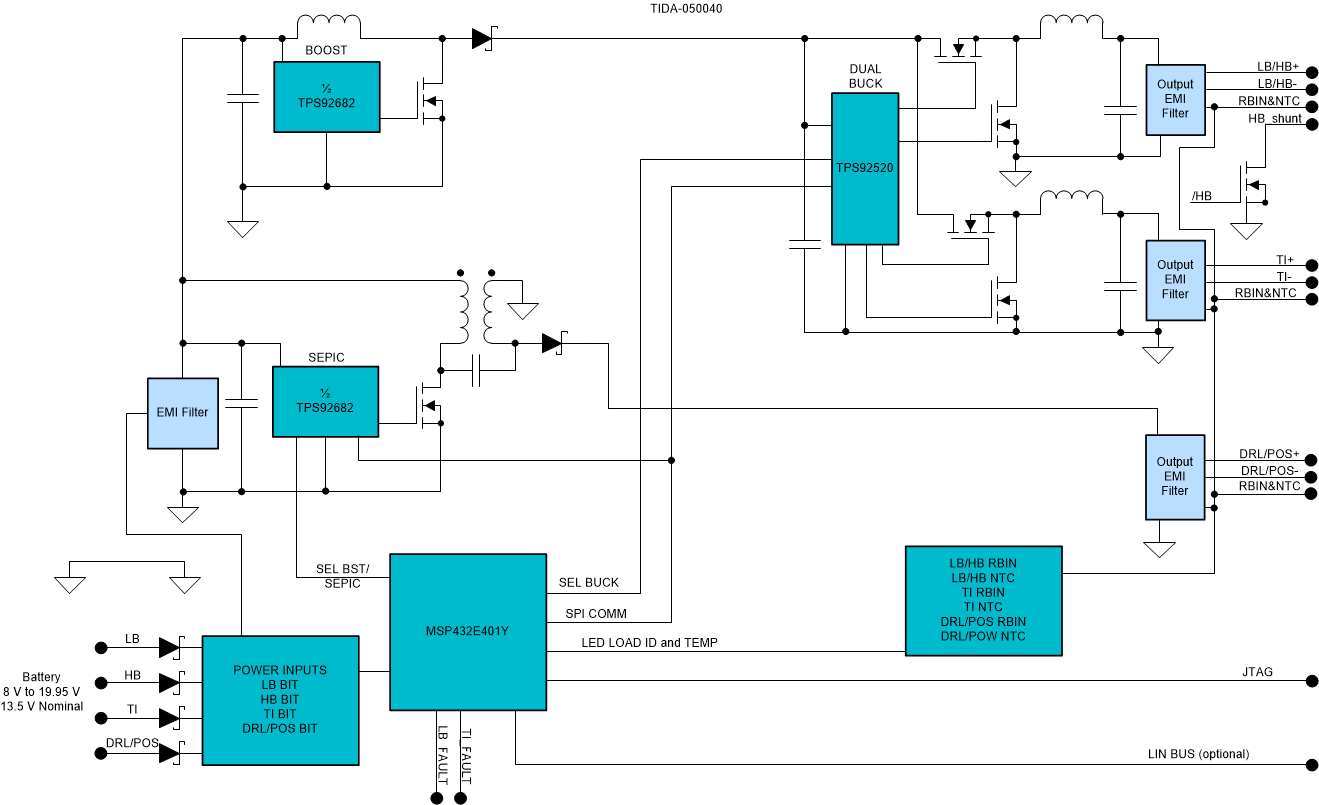
2.1 Block Diagram
 Figure 2-1 TIDA050040 Block Diagram