JAJU793 October 2020
- 概要
- リソース
- アプリケーション
- 特長
- 5
- 1System Description
- 2System Overview
-
3Hardware, Software, Testing Requirements, and
Test Results
- 3.1
Hardware Requirements
- 3.1.1 Getting Started
- 3.1.2 Testing and Results
- 3.1
Hardware Requirements
- 4Design and Documentation Support
2.2.2 Current Sensing Amplifier Design Overview
INA302-Q1 feature a high common-mode current sensing amplifier and two high-speed comparators. The two high-speed comparators have adjustable over current thresholds that are independent of each other enabling the ability to detect currents that are out of range. The response of comparator 1 is under 1µs and the alert response of comparator 2 is set through an external capacitor on the delay pin ranging from 2µs to 10s. Equation 1 provides a way to determine the delay response of comparator 2 based on the capacitor value chosen. Values for and are typically 1.22 V and 5 µA respectively.
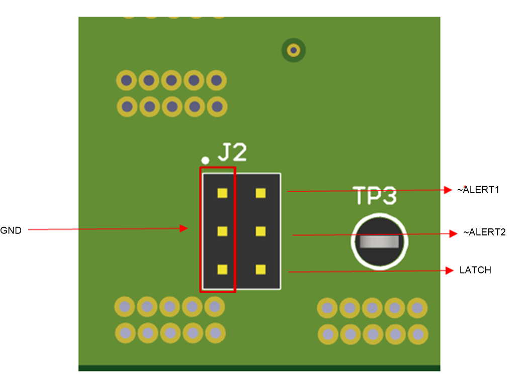
The design has a default of 470pF resulting in a of roughly 117 µs. INA302 has two modes available for the comparators based on whether the LATCH pins are pulled high or low. When the LATCH pin is low, INA302 is in transparent mode where the ALERT pins will follow the current sensed at the inputs. As such the ALERT pins will go back to normal if the current falls below the overcurrent threshold. When the LATCH pins are pulled high, the INA302 is in latched mode and once overcurrent is detected the ALERT pins will give an overcurrent signal until the LATCH pins are toggled to reset the ALERT pins. Latched mode is ideally used with an MCU that can toggle the LATCH pins low for at least 100ns.

Equation 2 provides a way to determine the resistor value needed on the LIMIT pins to get the desired current threshold value. The GAIN value for the INA302A2 device used is 50 V/V and is typically 80 µA. The design has a default a 1mΩ current sense resistor, a value for both LIMIT1 and LIMIT2 pins of 37.4KΩ to get a roughly 60A.

 Figure 2-5 TIDA-020040 Design J2 Connectors.