JAJU793 October 2020
- 概要
- リソース
- アプリケーション
- 特長
- 5
- 1System Description
- 2System Overview
-
3Hardware, Software, Testing Requirements, and
Test Results
- 3.1
Hardware Requirements
- 3.1.1 Getting Started
- 3.1.2 Testing and Results
- 3.1
Hardware Requirements
- 4Design and Documentation Support
2.2.1 Ideal Diode Design Overview
LM74810-Q1 is an ideal diode controller that drives and controls external back to back N-Channel MOSFETs. The first MOSFET to replace a Schottky diode and the second MOSFET allows load disconnect switch control. LM74810-Q1 has a wide input supply 3 V to 65 V, ideal for protection and control of 12 V automotive battery systems. Through controlling the MOSFETs, LM74810-Q1 provides reverse input protection, Reverse current blocking, in-rush current control, and adjustable over voltage protection.
TIDA-020040 controls two sets of MOSFETs in parallel to aid in decreasing power dissipation from the MOSFETs Rdson at high currents.
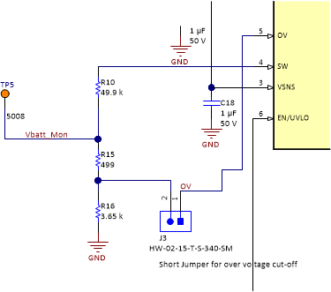
Adjustable over voltage protection is controlled through a resistor divider and connection to the OV pin of LM74810-Q1 which goes to an internal comparator with a set 1.23 V reference. When the voltage applied to OV is higher than the 1.23 V reference, overvoltage is triggered.
The design allows shorting J1 connector for over voltage clamping or shorting J3 connector for over voltage cut-off. For both connections, the resistor divider is the same to allow over voltage to trigger at 18.2 V.
 Figure 2-4 Over Voltage Resistor Divider
Schematic