JAJU793 October 2020
- 概要
- リソース
- アプリケーション
- 特長
- 5
- 1System Description
- 2System Overview
-
3Hardware, Software, Testing Requirements, and
Test Results
- 3.1
Hardware Requirements
- 3.1.1 Getting Started
- 3.1.2 Testing and Results
- 3.1
Hardware Requirements
- 4Design and Documentation Support
3.1.2.3 ISO7637-2 Pulse 1
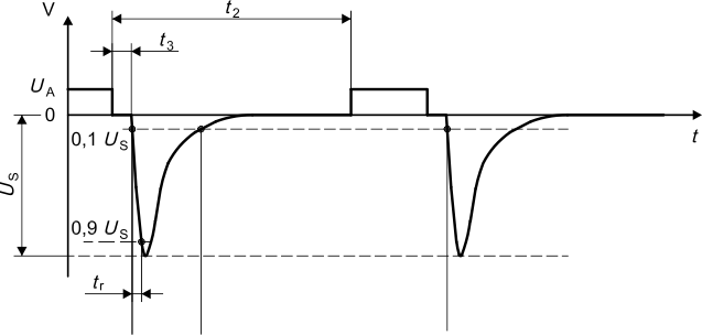
ISO7637-2 Pulse 1 test consists of battery disconnection where the voltage goes to zero volts and followed by -100 V. Figure 3-3 shows the typical waveform as well as the parameters for the test performed. The LM74810 should prevent reverse current as well preventing the output voltage from going negative in order to protect the rest of the circuit. Proper TVS selection performs a large role in the test to ensure the negative voltage is clamped within the 85 V operating maximum voltage across cathode to anode of the LM74810 as well as not exceed the of the 60 V MOSFETs.
- Us: 100 V
- Rise Time tr: 1us
- Output Resistance: 10 Ohms
- Pulse Width td: 2ms
- T2: 200ms
 Figure 3-3 ISO7637-2 Pulse
1
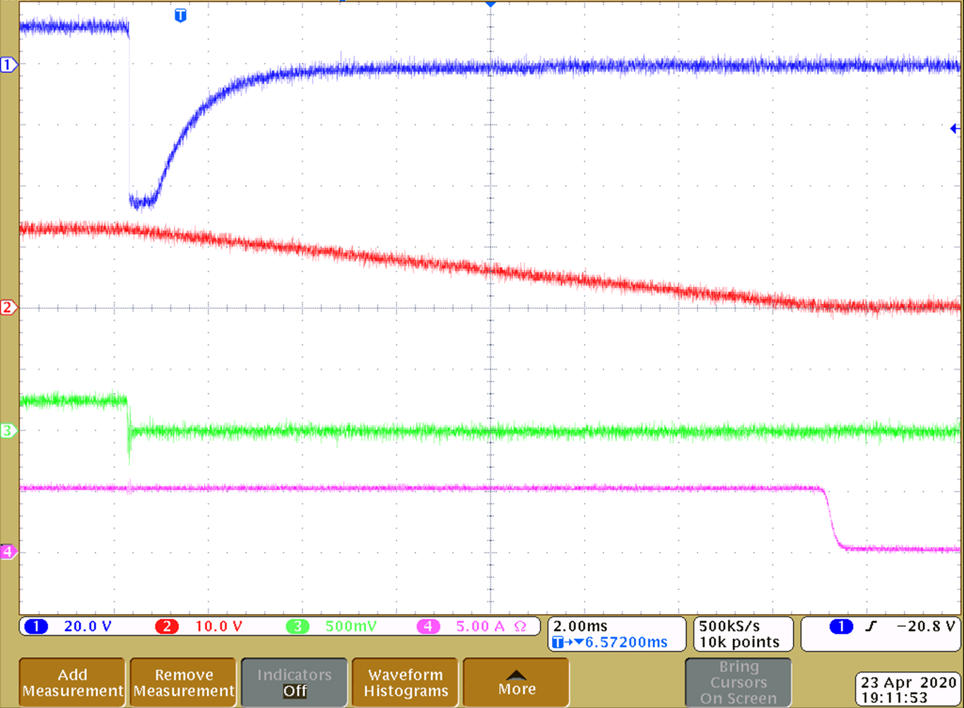
 Figure 3-4 ISO7637-2 Pulse 1
Test
Figure 3-4 ISO7637-2 Pulse 1
TestAs shown in Figure 3-4, the yellow trace is the input voltage which goes negative and the TVS diode clamps the input at roughly -45 V. The blue trace is the output which decreases and the green trace is the output current to the e-load which continues to draw current until the output goes to 0 V. The pink trace is the INA302 output.