JAJU793 October   2020


  1.   概要
  2.   リソース
  3.   アプリケーション
  4.   特長
  5.   5
  6. 1System Description
    1. 1.1 Key System Specifications
  7. 2System Overview
    1. 2.1 Block Diagram
    2. 2.2 Design Considerations
      1. 2.2.1 Ideal Diode Design Overview
      2. 2.2.2 Current Sensing Amplifier Design Overview
      3. 2.2.3 OR Gate Design Overview
      4. 2.2.4 MOSFET Selection
        1. 2.2.4.1 Blocking MOSFET
        2. 2.2.4.2 Hot-Swap MOSFET
      5. 2.2.5 TVS Input Diode Selection
      6. 2.2.6 Inrush Current
    3. 2.3 Highlighted Products
      1. 2.3.1 LM74810-Q1
      2. 2.3.2 INA302-Q1
  8. 3Hardware, Software, Testing Requirements, and Test Results
    1. 3.1 Hardware Requirements
      1. 3.1.1 Getting Started
      2. 3.1.2 Testing and Results
        1. 3.1.2.1 Over-Voltage Protection Cut-Off Mode
        2. 3.1.2.2 Over-Voltage Protection Clamping-Mode
        3. 3.1.2.3 ISO7637-2 Pulse 1
        4. 3.1.2.4 Overcurrent Protection
        5. 3.1.2.5 Load Dump
        6. 3.1.2.6 Cold Crank, Warm Start, and Cold Start
          1. 3.1.2.6.1 Cold Crank
          2. 3.1.2.6.2 Warm Start
          3. 3.1.2.6.3 Cold Start
        7. 3.1.2.7 Standby Current
        8. 3.1.2.8 Currency Sense Accuracy
  9. 4Design and Documentation Support
    1. 4.1 Design Files
      1. 4.1.1 Schematics
      2. 4.1.2 BOM
    2. 4.2 Documentation Support
    3. 4.3 サポート・リソース
    4. 4.4 Trademarks
Cold Start

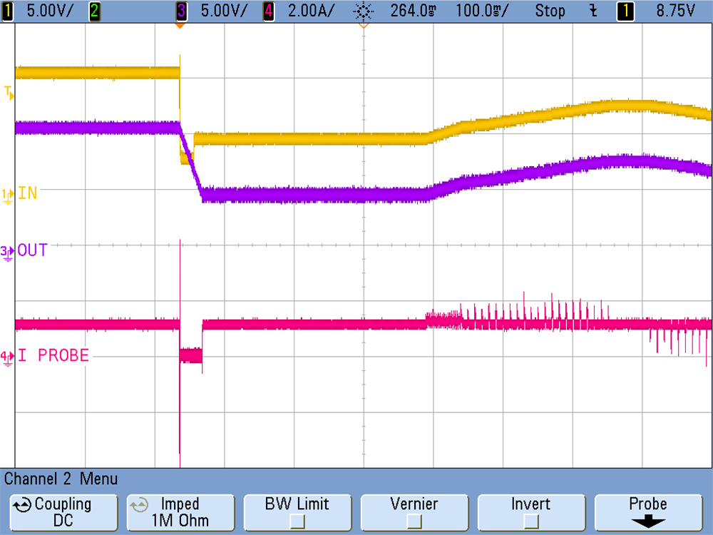
Cold Start is performed in a similar fashion as the cranking pulse tests shown before. Waveform seen at the input is shown in Figure 3-15. A drop of current is shown in Figure 3-16 as the blocking MOSFET turns off to prevent reverse current from flowing.
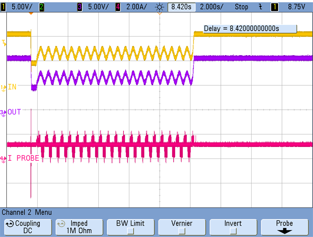
GUID-20200710-SS0I-QKGB-D4TS-7XMLNTSPRLHL-low.png Figure 3-15 Cold Start Waveform
GUID-20200710-SS0I-V8V6-K8FP-1CZTCDCXDXTT-low.png Figure 3-16 Cold Start Testing