JAJU793 October 2020
- 概要
- リソース
- アプリケーション
- 特長
- 5
- 1System Description
- 2System Overview
-
3Hardware, Software, Testing Requirements, and
Test Results
- 3.1
Hardware Requirements
- 3.1.1 Getting Started
- 3.1.2 Testing and Results
- 3.1
Hardware Requirements
- 4Design and Documentation Support
2.1 Block Diagram
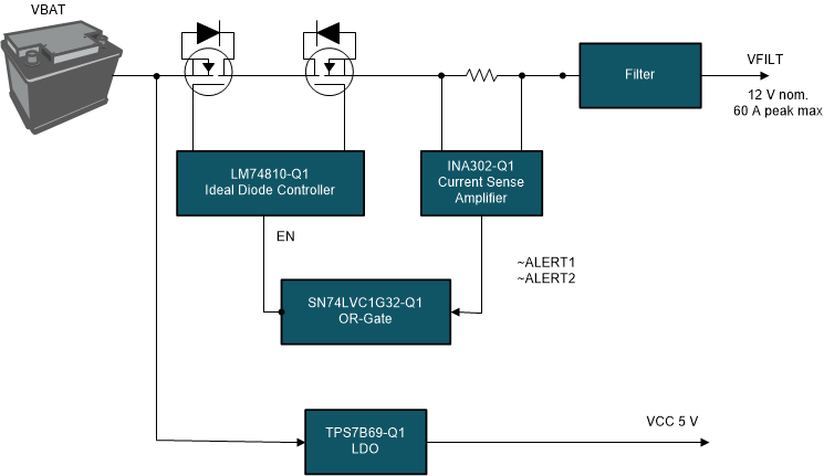
The block diagram for the design is shown in Figure 2-1. INA302-Q1 provides an analog current measurement output to be read by a microcontroller as well as two active low comparator outputs to signal if the current is above the threshold set. The two active low comparator thresholds can be independently set and one of the comparators can be set to have a delay through an external capacitor. The two comparator outputs serve as the inputs for the OR-gate which drives the enable signal for LM74810.
Connecting the overcurrent signal to the enable pin of LM74810 allows off turning off the ideal diode controller when there is an overcurrent condition. Using both comparator outputs of INA302 along with the OR-gate provides flexibility in how the comparator outputs are used. Using both comparators at different thresholds can provide a warning signal for sustained high current before reaching the overcurrent threshold as well as allow short current transients without triggering a fault condition. LM74810 drives back to back N-channel MOSFETs enabling reverse polarity protection, reverse current blocking, in-rush current control, and overvoltage protection. TPS7B69 is an LDO that provides the INA302 and the OR gate with a 5 V VCC from the battery voltage.
 Figure 2-1 TIDA-020040 Block Diagram